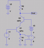
Well I still have to disagree with you guys on this one. Is there some "error current" being fed back to the emitter of the input device? Well, yahbut.....The "error current" is so small that it really isn't an important part of what is happening here. Let's plug in some numbers and see:
The current sources set up a standing current of about 5.5 mA in the input stage. This develops a bias voltage for the second stage of about 3 volts across the 560 ohm resistor. The emitter resistor of 100 ohms means that there will be a standing current of around 23 mA in the second stage. In Hawksford's tests he went for an output signal of 80 V p-p. Since the load resistor is 10 kohms, the signal current is +/- 4 mA.
So now can see that (regardless of whether the circuit is common emitter, standard cascode, or "enhanced" cascode), the voltage across the 100 ohm emitter resistor will vary between 1.9 V and 2.7 V.
In the case of the common emitter stage, the collector is swinging +/- 40 volts, so we can pretty much ignore the variation in emitter voltage when looking at how the Early effect impacts the performance of the circuit.
Now let's look at the standard cascode. Assuming 1.9 V per LED, the collector voltage of the cascoded transistor is clamped at 3.1 V. But now the signal swing at the emitter becomes critical. Throughout the signal swing, Vce will vary between 0.4 V and 2.2 V.
We have to pay attention to this very closely. In the first place we will see some Early effect from this voltage swing. Secondly, when the transistor has only 0.4 V across it, we will be dropping down below the "knee" of the characteristic curves and generating some non-linearities. In contrast, the "enhanced" cascode keeps a constant 1.2 V across the cascoded transistor. And this increased stabilization of operating point is the real reason why the "enhanced" cascode measures better.
Looking at the contribution of the "error current" proposed by Hawksford, let's assume that the beta of the cascode transistor is 100. That means that the "error current" fed back by the base of the cascode will be +/- 40 uA. This "error current" signal is fed to the junction of a 100 ohm resistor and the emitter of the cascoded transistor. Now the impedance of the emitter will be about 1.1 ohms with a standing current of 23 mA. So the "error current" will generate an "error voltage" of around 40 uV.
From the Ebers-Moll equation we know that a 40 uV change in Vbe will result in a change in collector current of around 0.1% or so. This is just not a dominant mechanism in this circuit. The real increase in measured linearity comes from a more "cascode-like" cascode, since the operating point of the cascoded transistor is stabilized to a greater degree.
Attachments

Note to flaming threadsters. This is the way gentlemen conduct themselves in a healthy debate. A few members could take a lesson from these guys.
Interesting stuff!😉
Interesting stuff!😉
Have to agree with you there. Excellent stuff!
Charles,
I have a question, should the 3.9k (attached to zeners) resistors be attached to ground or each other, rather than the output(or 10k resistor) or am I reading the schematic incorrectly?
Regards,
Jam
Charles,
I have a question, should the 3.9k (attached to zeners) resistors be attached to ground or each other, rather than the output(or 10k resistor) or am I reading the schematic incorrectly?
Regards,
Jam
Hello Jam,
Sorry, I had to reduce the resolution of the image to get the DIY website to accept it. There is no other connection at the junction of the two 3.9 k resistors. By symmetry, they could go to ground. The 10 k resistor is a load for the output stage.
By the way, this circuit is actually on-topic with the original point of the thread -- more zero-feedback circuits. In Hawksford's paper he shows it in three variants:
1) The "enhanced" cascode as I posted (cascode referenced to the cascoded transistor's emitter).
2) Regular cascode, where the cascode is referenced to the supply rail by two LEDs instead of the one shown in the posted figure.
3) Common emitter, where the cascodes are removed altogether.
The input impedance is rather low, and you would need to add current gain to drive speakers, but not a bad circuit.
Best regards,
Charles Hansen
Charles,
Could you not attach the junction of the emitter resistors (input) and drive the bases of the input transistors. If so how would this change the performance?
Regards,
Jam
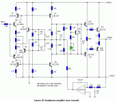
More food.....................😉 (As usual ignore the servo........I hate those things)
Could you not attach the junction of the emitter resistors (input) and drive the bases of the input transistors. If so how would this change the performance?
Regards,
Jam
More food.....................😉 (As usual ignore the servo........I hate those things)
Attachments
Jam,
You can do anything you want to do! 😀
Hawksford didn't do that because he was trying to show the improvement in linearity by cascoding. If he had driven the bases of the input transistors, this non-cascoded stage would have swamped the effects he was trying to show.
I like your last circuit a lot. Where is this from?
Charles Hansen
OK, I found the circuit:
http://hjem.get2net.dk/bencar/kumisa/k3/KumisaIII_headwize.html
The author had this to say:
"I must admit that I used one of the best opamps on the market and still I get better results using ordinary transistors and no feedback. Now I'm thinking about changing my RIAA circuit to a non-feedback design, instead of using the OPA2134 and AD812."
which is consistent with my experience, and the reason for this thread.
It was Wilde
"Could you not attach the junction of the emitter resistors (input) and drive the bases of the input transistors. If so how would this change the performance?"
Significantly......... since there wound be no bias for the input transistors! Actually it looks like Q5 and Q6 are the diff pair for the negative feedback. Where do you find this stuff? I'll bet you enjoyed puzzles as a child.😀 It gives me a headache trying to figure it out. Anybody want to guess the closed loop AC gain? My guesstimate is about 2.65 after a pretty quick look at the schematic.
"Could you not attach the junction of the emitter resistors (input) and drive the bases of the input transistors. If so how would this change the performance?"
Significantly......... since there wound be no bias for the input transistors! Actually it looks like Q5 and Q6 are the diff pair for the negative feedback. Where do you find this stuff? I'll bet you enjoyed puzzles as a child.😀 It gives me a headache trying to figure it out.
Anybody want to guess the closed loop AC gain? My guesstimate is about 2.65 after a pretty quick look at the schematic.Fred, you're slipping! 🙂
Jam's question was in reference to the schematic I posted, not the schematic he posted.
Regarding the schematic he posted, Q5 and Q6 not providing feedback. Look at the horizontal wire going down the middle -- it's connected to ground.
Jam's question was in reference to the schematic I posted, not the schematic he posted.
Regarding the schematic he posted, Q5 and Q6 not providing feedback. Look at the horizontal wire going down the middle -- it's connected to ground.

dimitri said:Is it something to be proud of?
OK, since Dimitri isn't elaborating and nobody else is leaping to
my defense, I will point out that my patent #3,995,228 was
invented in 1974 and patented in 1976.
Malcolm Hawksford's paper presenting a similar circuit "Reduction
of Transistor Slope Distortion in Large Signal Amplifiers" was
published in April 1988. It was followed shortly therafter by
Cordell's version.
I assume that Dimitri is confusing this with the earlier discussion
of a different circuit relating to folded cascode.
Welcome to Jamaica, Mon, and have a nice day. 😎
Oy, I should live so long.....
"Yeah! It must be old age getting to Fred .................."
That's funny he was nice on the phone 30 minutes ago.😕 Alright ...... I will look into 300mA for the shunt regulator. Maybe a dual footprint for an alternate Hitachi mosfet would do it. I know extortion when I see it.
"Yeah! It must be old age getting to Fred .................."
That's funny he was nice on the phone 30 minutes ago.😕 Alright ...... I will look into 300mA for the shunt regulator. Maybe a dual footprint for an alternate Hitachi mosfet would do it.
I know extortion when I see it.Nelson Pass said:OK, since Dimitri isn't elaborating and nobody else is leaping to
my defense, I will point out that my patent #3,995,228 was
invented in 1974 and patented in 1976.
Malcolm Hawksford's paper presenting a similar circuit "Reduction
of Transistor Slope Distortion in Large Signal Amplifiers" was
published in April 1988. It was followed shortly therafter by
Cordell's version.
I assume that Dimitri is confusing this with the earlier discussion
of a different circuit relating to folded cascode.
Leaping to someone's defense? OK, I'm game! 🙂 Well, maybe it's more a case of minding the Ps and Qs.
It doesn't change your point, Nelson, but the Hawksford paper that proposed a variation on your patent #3,995,228 was actually "Distortion Correction Circuits for Audio Amplifiers," 1981 July/Aug. So you beat him to the punch there.
The Hawksford paper you noted had the idea for operating the input transistor and cascode at different bias currents as in your later patent #5,343,166.
Nelson Pass said:Thanks for the correction - I swapped my titles.
You mean mixing up the audio designer Pass with the oenologist
Pass?? 😉
Just joking.
Charles Hansen said:The current sources set up a standing current of about 5.5 mA in the input stage. This develops a bias voltage for the second stage of about 3 volts across the 560 ohm resistor. The emitter resistor of 100 ohms means that there will be a standing current of around 23 mA in the second stage. In Hawksford's tests he went for an output signal of 80 V p-p. Since the load resistor is 10 kohms, the signal current is +/- 4 mA.
So now can see that (regardless of whether the circuit is common emitter, standard cascode, or "enhanced" cascode), the voltage across the 100 ohm emitter resistor will vary between 1.9 V and 2.7 V.
Well, I'm not sure where to start with this, so let's look at the biasing. First, the DC current in the input current sources is about 5.33 mA. For the 3.9k resistors, their current is about 0.15 mA. This subtracts from, rather than adds to, the input stage current, giving a result of about 5.18 mA (since the emitter voltage of the input NPN is negative). This gives a voltage drop across the 560 Ohm resistor of about 2.9 Volts. So the VAS emitter resistor has about 2.2 Volts across it, giving about 22 mA. For an output voltage of 40 Volts peak, the current of the upper half of the VAS increases by 2 mA from its quiescent value, while that of the lower half decreases by 2 mA, and the opposite for -40 Volt output of course. This requires that the voltage drop across the 100 Ohm resistor change by +/- 0.2 Volts, or a range of 2.0 Volts to 2.4 Volts. So you've neglected the push-pull nature of the circuit when you calculated double that swing across the resistor as 1.9 to 2.7 Volts. Assuming the collector of the cascoded transistor is clamped at 3.1 Volts from the rail, then its Vce value is a minimum of 0.7 Volts, rather than 0.4 Volts. This is about the same as Vbe, so the collector-base voltage is very near zero, giving the possibility of increased distortion. Yet this doesn't seem to prevent it from having a factor of ten less distortion than the CE amp at 1 kHz.
Charles Hansen said:(...)Looking at the contribution of the "error current" proposed by Hawksford, let's assume that the beta of the cascode transistor is 100. That means that the "error current" fed back by the base of the cascode will be +/- 40 uA. This "error current" signal is fed to the junction of a 100 ohm resistor and the emitter of the cascoded transistor. Now the impedance of the emitter will be about 1.1 ohms with a standing current of 23 mA. So the "error current" will generate an "error voltage" of around 40 uV.(...)
The error voltage in this case isn't really relevant though. Only the current need be considered. Since you have a very low impedance looking into the emitter compared to the 100 Ohm emitter resistor, and by your own assumption can invoke linearity here, then simple current division says that virtually all of the error current will circulate back into the emitter of the common emitter amp. Then multiply this change in emitter current by the transistor alpha to get the change in collector current. So the only scaling we see of this error current is the current division between the 100 Ohm emitter resistor and the impedance looking back into the emitter of the common emitter amp, and the alpha (= beta / (beta + 1)) of the common emitter amp. Therefore the correction current added at the emitter of the common base amp is almost exactly the same as its base current Ierr (specifically (alpha_CE * 100 / (100 + re)) * Ierr) which is exactly what we want.
Also, the estimate of the base current of the common base amp must increase at high frequencies due to its collector base capacitance. This current also contains distortion due to the modulation of the collector-base capacitance value over the full output swing of the amp. It's the cancellation of this distorted current that causes the reduction of the distortion at high frequencies (relative to the conventional common base amp) to be more than at low frequencies. The argument you've presented regarding voltage swing has no inherent frequency dependence and therefore doesn't explain why the distortion reduction is better at higher frequencies than low.
If you really believe this is a biasing issue, you can do a SPICE simulation by altering the enhanced cascode so the base bias of the common base amp is derived from a unity gain ideal VCVS connected to the emitter of the common emitter amp, with an ideal DC voltage source in series with it to bias the base of the common base amp. This will give the same "more cascode-like behavior" (AKA reduction of the Early effect which you claimed earlier to not be of any relevance 🙂 ) to the cascode, yet prevent any error current from getting back into the emitter of the common emitter amp. This will give higher distortion than the enhanced cascode. This would need to be run with large voltage swings to demonstrate the effect. An example is below, though Hawksford's circuit is simple enough for a fairly quick sim.
Attachments
Andy,
Thanks for the very detailed and well thought out post. You are correct that I neglected to account for the push-pull action in my earlier analysis. I agree with the rest of your analysis as well. The way I would summarize the whole thing is as follows:
1) The low-frequency linearity of a degenerated common-emitter stage is actually quite good. However, at large signal swings the load line intersects the "knee" of the characteristic curves, causing increased distortion. This effect can be avoided by using a steeper load line. A cascode connection provides a very steep load line, and can give an improvement for large signal swings.
2) The input capacitance of a common-emitter stage is somewhat non-linear, especially at high signal swings. If the CE stage is driven from a high source impedance, this will cause added distortion at high frequencies. Cascoding is one technique that can linearize the input capacitance of the CE stage, thereby reducing HF distortion if the source impedance is high.
3) Referencing the cascode to the emitter of the CE stage ("enhanced" cascode) provides two additional distortion reduction mechanisms. At low frequencies the load line is significantly steeper than a cascode referenced to ground, as value of the emitter resistor is effectively removed from the load line. At high frequencies, the effect of non-linear capacitances from the cascode itself is mitigated by a feedback path to the CE stage.
I think that covers everthing that both you and I have said. 🙂
Now I'm wondering if anyone can tell us why the consensus seems to be (at least on this thread) that the poorer-measuring normal cascode sounds *better* than the better measuring "enhanced" cascode?
Or perhaps even more interesting, why *any* cascode degrades the sound (according to another thread here?
Best regards,
Charles Hansen
what about a cascoded current source ?
So it seems like jury is out on the cascode that is directly in the signal path. Some think there is an improvment others think there is a price to pay that is too high.
But what about the cascode in a current source ( which, in one way of looking at it, is one step removed from the signal path )
Has anyone noticed that the cascode has any negative effect in this role ?
OK, since Dimitri isn't elaborating
Wouldn’t like to be a “flaming threadster” so please let me continue in private …
- Status
- Not open for further replies.
- Home
- Amplifiers
- Solid State
- Another Zero Feedback Amplifier