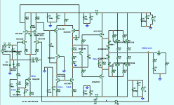
lee , your amp looks a lot like mine. I have run IRF's on mine in the real world and it works. Your bode plots lack sufficient open loop gain and are a bit undercompensated. Your amp might not outright break out into oscillation , BUT , with those voltages and 10 pair OP's , I'd be careful. The KSA1381/KSC3503 gaingroup E or F will get you that 70DB open loop gain . Drivers don't work well for a VAS.
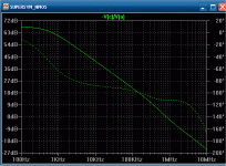
Below is the amp as I had it and the loop gain as it should be. I only used 2 pair. You should build with 1 pair , test it out at low power / w - scope. Then run full monty. what is below works , holton's amp was the role model.
OS
Below is the amp as I had it and the loop gain as it should be. I only used 2 pair. You should build with 1 pair , test it out at low power / w - scope. Then run full monty. what is below works , holton's amp was the role model.
OS
Attachments
Hi Piersma
No, I haven't built any boards yet. 😱 Shame on me. 😱
This is for two reasons:
1. I don't feel fully comfortable with grounding yet. I consulted prairiemystic who confirmed the layout isn't bad altogether 😉 and gave me some valuable advice. (Thanks!!!) I thought about grounding again but didn't find a solution that makes me really happy.
I'm struggling between the ground as is (just with all the AGND joined on PCB instead of being divided in two like on the preview PCB) and a small ground plane for the AGND section. I always use ground planes at work with various digital stuff and it works well. But this is different. I'm afraid a ground plane could introduce unpredictable parasitic capacitance that could upset the amp somehow. What do you think?
2. It's summer now. 🙂 🙂 🙂 After the long, cold and rainy "spring" I enjoy the great weather now and don't find the time to work on the project.
However this is a good opportunity to thank you for contributing so much to this project. Without you I'd have built "another AV800/AV1000". You took this project far beyond what I expected to turn out.
I will finish this amp for sure but not right now. I will continue as soon as seasons start to change. I already foresaw I won't find the time to work on the project in summer and I was right.
Great to see you're still interested in the project. Please stay tuned. 🙂
Hi ostripper
Yes, your amp is VERY similar to the one we designed. Since yours work I'm confident mine will work, too. 🙂 Thank you very much for warning and the optimal bode plot. I'm glad I bought the F gain group of the KSA1381/KSC3503. I will follow your advice for testing the amp.
Best Regards
Lee
Routing
hi Lee,
I like the way you routed the AGND and the real small groundplane you created on the PCB bottom, it will work o.k.
The DGND plane is maybe a little overdone, but i don't think it will create problems. If you wish you could reduce the DGND plane, but let it exist under the Hs1/Hs2 heatsinks.
Enjoy the summertime!
regards,
Piersma
Hi all
I noticed Ostripper wasn't lazy like me and designed a great amp in the meanwhile. 😉
http://www.diyaudio.com/forums/solid-state/169590-mongrel-supersym-ii.html
@ Ostripper:
Since you are a *sym expert maybe you like to help me a bit? 😉
What is your suggestion to improve compensation?
I wonder what is the difference/ advantage / disadvantage between connecting the casode stage Zener (D8 in your schematic above) diode to either ground or the tail CCS. 😕 Piersma brought this up before...
You put diodes in series with the output stage gate Zener clamping diodes. What is the advantage to do so?
In the Mogrel thread Lineup proposed to use a current mirror in the input stage (post 151). I simulated this some time ago and dismissed. 😱 Is there a chance for improvement?
Best Regards
Lee
Attachments
Hi all
I noticed Ostripper wasn't lazy like me and designed a great amp in the meanwhile. 😉
http://www.diyaudio.com/forums/solid-state/169590-mongrel-supersym-ii.html
@ Ostripper:
1.Since you are a *sym expert maybe you like to help me a bit? 😉
2.What is your suggestion to improve compensation?
3.I wonder what is the difference/ advantage / disadvantage between connecting the casode stage Zener (D8 in your schematic above) diode to either ground or the tail CCS. 😕 Piersma brought this up before...
4.You put diodes in series with the output stage gate Zener clamping diodes. What is the advantage to do so?
5.In the Mogrel thread Lineup proposed to use a current mirror in the input stage (post 151). I simulated this some time ago and dismissed. 😱 Is there a chance for improvement?
Best Regards
Lee
questions??? 😕 I am not the only expert here , but here goes.
1. I an glad to be of assistance.
2.What you see on my last post is ideal ,it worked with the IRF's and the BJT's. What you propose with the HUGE array of arc welding MOSFETS should be prototyped and tested,tested ,and tested with just 1 pair, ...
 BEFORE you extend it to 10 pair.
 3.For an unregulated input stage PS , the zener is best. I now use a full capacitance multiplier or at least a CRC filter between the output stage and the VAS/LPT. For an amp of this caliber , I would consider fully separate supplies.
4. This is standard, look here....Project 101 - High Power, High Fidelity MOSFET power amplifier
and this is the "way" on just about my whole lateral/vertical mosfet project collection.
5.A current mirror is worth consideration if you use a FET input pair at low Ic... the loop gain is too low and a CM doubles what you have.
OS
Hi Ostripper
1. 🙂 🙂 🙂 Thank you very much. 🙂 🙂 🙂
2. You were right: The amp was totally undercompensated. I didn't care about compensation and just used the one from the AV amp. Now it's much better.
3. I already split supplies so that I can use separate supplies later. For testing I will use a common supply. What I liked to ask about the Zener was the Anode connection. In the Symasym and Mongrel amp the Anode is connected to the tail current source. In the AV amp it is connected to ground. I simulated both versions PSRR and was surprised the ground connected one seems to have much better PSRR. Maybe I'm wrong. Can you confirm this? I attached plots of both versions.
The file named amp-simulation_casc-ccs2_swcm_BJT-drv_FET-bias_save-bias_VAS-tran_-_inpPSRR is the version with the Anode connected like in the *sym amplifiers and the amp-simulation_casc-ccs_swcm_BJT-drv_FET-bias_save-bias_VAS-tran_-_inpPSRR is the AV style connection. (Btw: Sorry for the lengthy file names. 😉 )
4. Ok, agree. I will do it this way.
5. So the input current mirror seems to be of little usefulness here. I anyway had no board space left for it but was just curious.
6. In the Symasym and Mongrel amps the VAS is loaded with resistors and sometimes capacitors, too. (Not in the version you posted above) When I simulated this it always spoiled my THD. What is the reason for such VAS loading? Maybe improved stability?
Best Regards
Lee
Attachments
Last edited:
#6 - loading the vas with resistance/capacitance.Resistance affects (reduces)the total loop gain of the amp and changes the harmonic structure of the residual distortion components. Using shunt capacitance at the VAS effects the unity gain point(UG) , phase margin, and the high order harmonics. You won't burn the amp "playing" with these values but they do affect the overall "character" of the resulting sound.
OS
OS
Thanks for the explanation.
3. While it seems correct that junk from the positive supply is injected to the LTP emitter resistors node because of cascode CCS imperfection and is also flowing through the tail ccs the amount of current is small and seems not to affect the amp considerably. Thus I decided to connect the Zener anode to the LTP like in all Sym* amps.
After some minor changes I think the amp is ready for a prototype now.
I gave it a name since every amp needs a name:
official name is: Lee Knattas Weld-a-Sym
(inofficial name is: Piersmas Knattasym 😉 )
Layout has changed as well. I decided to replace all SMT capacitors with THT ones for reliability concerns. Although I soldered several thousands of SMT caps by hand and till now the boards are working I prefer THT caps here. The SMT parts were just habit. Hand soldering puts a lot of thermal stress on them and they might crack immediately or they might crack later because soldering weakened them or because of board flex. I'll keep the SMT resistors for space reasons and because they are less likely to be damaged during soldering and I can change them with the board mounted to the heat sinks.
I will order boards next week.
I'm still looking for a better way to post a preview here...
Again thanks to all who contributed here or in the other Sym* threads.
Best Regards
Lee
Attachments


Any changes on AV1000's original design
Hi Lee
Same as you, I am about to assemble AV1000. I already finished my schematic and struggling with PCB right now.
I found your PCB pretty good job, well done! however I cant use it as I have to go with single layer layout 🙁
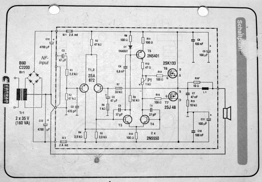
Just a question; I am using Anthony's version 3 (Below my schematic source) . Is there any major change that you found will be better to implement?
I'd appreciate if you can update me on that.
Hi Lee
Same as you, I am about to assemble AV1000. I already finished my schematic and struggling with PCB right now.
I found your PCB pretty good job, well done! however I cant use it as I have to go with single layer layout 🙁
Just a question; I am using Anthony's version 3 (Below my schematic source) . Is there any major change that you found will be better to implement?
I'd appreciate if you can update me on that.
Attachments
Hi keivanmh
I know my PCB design is useless for the DIY community and I'm sorry for that. I was thinking about releasing a DIY community version once my amp is running optimized for DIY needs but since I'm rather used to design four layer boards doing a single layer design would be hard for me. Maybe I'll try, don't know yet.
However, for the case you need help with your board design for your AV1000 I'd be happy to help.
Thanks for the schematic! 🙂 🙂 🙂
It is very interesting to see how Anthony's amp evolved.
What I would change?
(Note: This is not bashing Anthony! Just my opinion.)
In my opinion the way the bias is set with P1 is dangerous. When I found out how biasing works at all, the thought "What if the wiper loses contact?" came into my mind. In this case the output stage might receive bias way too high and might be destructed. D. Self confirmed my concerns in his power amplifier book.
That's why I implemented the biasing scheme that is used in most amp schematics I've seen. It should work in the AV1000 as well.
That's the only thing I'd recommend to change.
The other changes recommended to me or stolen from other *sym amps are optional.
My swapped Wilson current mirror is most likely just useless.
Note that your C7 needs to be a mica cap.
I recommend an output inductor parallel with a resistor after the Zobel network (R68, C32) in series with the speaker as seen in many amplifiers (see attached schematic). The inductor could be something like 1 uH to 3 uH and the resistor 4R7 to 10R maybe.
By the way: How do you like my DIY output inductors?
It was very hard to find small coil formers. (That's why there wasn't any progress for some time...) They measure 12mm diameter and 30mm length. I used 1,5mm diameter wire. Inductance is 3 uH, series resistance 10 mOhm. The inductor design is a compromise between size and performance.
Best Regards,
Lee
Attachments

Hi all
Cleaning up my design directory I stumbled across the schematic of the amp I built maybe 10 years ago. I just took a photo and posted it here:
http://www.diyaudio.com/forums/solid-state/166212-amp-circuit-2sj50-2sk135-2.html
But didn't notice that the amp also has a topology similar to the *Sym ones. Funny, isn't it? 🙂
Just because I'm curious I simulated the schematic and was surprised it didn't sim as bad as I expected.
Best Regards,
Lee
Attachments
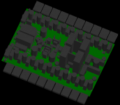
I finished board layout today and will order boards tomorrow (this time for sure). 😀
Attached is a preview of the final board layout.
The 3D view is nice to have but pretty useless since I cannot export to 3D CAD formats.
Attached is a preview of the final board layout.
The 3D view is nice to have but pretty useless since I cannot export to 3D CAD formats.
Attachments

Hi Lee,
Nice final PCB, where are the boards going to be produced?
I am curious about the pricing.......
regards,
Piersma
Nice final PCB, where are the boards going to be produced?
I am curious about the pricing.......
regards,
Piersma
Hi Piersma
The boards will be manufactured in the UK afaik.
I ordered five boards (MOQ) and each costs me 48 Euro.
I decided to have 70 um Cu for lower resistance since this isn't expensive. Pads will be standard pb free HASL. I could have had silkscreen for free but have no space left for any. I thought about 2mm FR4 but decided against because I have no experience with it and don't like to experiment with it right now.
Best Regards,
Lee
matching HEXFETs
Today I matched the HEXFETs.
For the test circuit I used a 15V voltage supply, three huge 25W resistors in series gave 118 Ohm and a good multimeter.
For the N-channel device the gate was connected to drain, source to ground, drain to +15V via resistor. Drain to source voltage was measured within two or three seconds and rounded to three digits since the last one is changing too fast. For the P-channel device gate was connected to drain, drain grounded and source connected to +15V via the resistor. Drain to source voltage was measured.
Source current was 90 mA.
This is the raw data showing deviation of values for the rails:
Maybe it's interesting for others who have to match their HEXFETs to see what can be expected when buying a rail of them.
IRFP240
Rail 1
3.99 ++
3.98 ++
3.97 +
3.96 +++++
3.95 ++++
3.94 ++++
3.93
3.92 +++
3.91 +
3.90 +
3.89 +
3.88
3.87
3.86
3.85
3.84
3.83
3.82
3.81 +
Rail 2
4.07 ++
4.06 +
4.05 +
4.04 +
4.03 ++++
4.02
4.01 +
4.00 +++++++
3.99 +++++
3.98 ++
3.97 +
Rail 3
4.05 +
4.04 ++
4.03 ++++
4.02 +
4.01 +
4.00 ++
3.99 +
3.98 +
3.97 +
3.96
3.95 ++
3.94 +++++
3.93 +++
3.92 +
Rail 4
4.00 ++
3.99 +++
3.98 ++++++
3.97 +++
3.96 +++
3.95 ++
3.94 +
3.93
3.92
3.91
3.90
3.89 +
3.88 +
3.87 +
3.86 +
3.83 +
IRFP9240
Rail 1
3.98 ++++
3.97 ++++
3.96 +++++++
3.95 ++++
3.94 +
3.93 ++++
3.92 +
Rail 2
3.94 +
3.93
3.92
3.91
3.90
3.89 ++++++++++
3.88 +++
3.87 ++++
3.86 ++++
3.85 +
3.84 ++
Rail 3
4.01 +
4.00
3.99 ++++++
3.98 +++++++++
3.97 +
3.96 ++
3.95 +++++
3.94 +
Rail 4
3.94 +
3.93 ++++++++++++
3.92 ++++++++
3.91 +++
3.90 +
Total:
IRFP240:
3.81 1
3.83 1
3.86 1
3.87 1
3.88 1
3.89 2
3.90 1
3.91 1
3.92 4
3.93 3
3.94 10
3.95 8
3.96 8
3.97 6
3.98 11
3.99 11
4.00 11
4.01 2
4.02 1
4.03 8
4.04 3
4.05 2
4.06 1
4.07 2
IRFP9240:
3.84 2
3.85 1
3.86 4
3.87 4
3.88 3
3.89 10
3.90 1
3.91 3
3.92 9
3.93 16
3.94 4
3.95 9
3.96 9
3.97 5
3.98 13
3.99 6
4.01 1
Holtron wrote in his paper to match the devices in groups of +-0.1V to +-0.2V. This must be a typo. I think it should read +-0.01V to +-0.02V.
Matching the BJTs will be much harder. I'm not looking forward to this.
Hi Lee
Back when I wrote the manual Matching the Hexfets to within 0.1v or 0.2 in practise seemed to work just fine.
These days I would match them to within 5mv of least, just to make sure.🙂
Cheers
Anthony
Aussie Amplifiers
Back when I wrote the manual Matching the Hexfets to within 0.1v or 0.2 in practise seemed to work just fine.
These days I would match them to within 5mv of least, just to make sure.🙂
Cheers
Anthony
Aussie Amplifiers
Hi Anthony
Thanks for clarification. 🙂
Matching them more closely than I did would be much more effort. I noticed the source current immediately starts to heat up the die and makes Vgs fall approx 1mV per second. I hope my FETs were at equal temperature before I started. 😉 Maybe it was better to match them at a much higher temperature but this would take many days...
Since the FETs matched to 0.1V worked fine for you and many DIYers who built AV amps I'm not too worried anymore.
Best Regards,
Lee
I finished board layout today and will order boards tomorrow (this time for sure). 😀
Attached is a preview of the final board layout.
The 3D view is nice to have but pretty useless since I cannot export to 3D CAD formats.
I use Eagle, Eagle 3D Povray. Many of the texts I wrote 3D Eagle
An externally hosted image should be here but it was not working when we last tested it.
- Status
- Not open for further replies.
- Home
- Amplifiers
- Solid State
- another one to build an AV800 / AV1000