I can tell that I waste my time today: I have a bad scope probe (one of the two). I have a strong high on G1 and a G2 that goes with phi1 because G2B goes with Phi1 of the 6875 and G2A its directly connected with ground, that seems good.
So at any clock time the eprom can be read I think
So at any clock time the eprom can be read I think
Hi.
G pins of 74138 decoder are enable pins, Yx outputs are based on the decoding of A,B and C inputs,this is what matters. So what you describe is that 74138 is enabled, thats OK.
A,B & C inputs are very likely connected like this :
2716 is a 2k*8 EEPROM (2516 is TI version of 2716) use 11 adresses lines; with only 3 decoded; EEPROM memory range will be repeated 4 times as two lines remains unused.
What matters is that EEPROM is readable from adresses $F800 to $FFFF because reset vector of 6800 is in $FFFE and $FFFF.
Checking for chip select and adress decoding is better made with analyser but after been sure that buses signal integrity is ok.
Without schematic and prior knowledge of the board best way to troubleshoot is going the hard way, by first checking the basics then slowly going trough the system, this test sequence is typically :
Supply
Reset
Clock and some controls signals
CPU activity then bus and control signal integrity on various circuit areas (pre / post buffers)
Adress decoding on RAM, ROM, peripherals
Then you can start to wonder if ROM or RAM is ok or try to understand what cpu is doing with mode advanced methods.
Chris
G pins of 74138 decoder are enable pins, Yx outputs are based on the decoding of A,B and C inputs,this is what matters. So what you describe is that 74138 is enabled, thats OK.
A,B & C inputs are very likely connected like this :
- C to A15 (Adress bus)
- B to A14
- C to A13
2716 is a 2k*8 EEPROM (2516 is TI version of 2716) use 11 adresses lines; with only 3 decoded; EEPROM memory range will be repeated 4 times as two lines remains unused.
What matters is that EEPROM is readable from adresses $F800 to $FFFF because reset vector of 6800 is in $FFFE and $FFFF.
Checking for chip select and adress decoding is better made with analyser but after been sure that buses signal integrity is ok.
Without schematic and prior knowledge of the board best way to troubleshoot is going the hard way, by first checking the basics then slowly going trough the system, this test sequence is typically :
Supply
Reset
Clock and some controls signals
CPU activity then bus and control signal integrity on various circuit areas (pre / post buffers)
Adress decoding on RAM, ROM, peripherals
Then you can start to wonder if ROM or RAM is ok or try to understand what cpu is doing with mode advanced methods.
Chris
Last edited:
Can you post picture of the board.
RAM looks like it's made of 2 chips of 2114, those are possible failure sources....
RAM looks like it's made of 2 chips of 2114, those are possible failure sources....
Hi Chris, many thanks for ypour suggestions and your help, here two pictures of the board:


in the next post I show you what I can measured on data and adress bus of the MCU
in the next post I show you what I can measured on data and adress bus of the MCU
following your suggestions on post #40 I put 0 on the lower line, scope DC coupled, 1 V/div, 2 uS/div (5 is the same:

A0, A1, A2 are quiet the same

A3, A5, A6

A7, A8, A9

A10

A11 to A15

BA

VMA
A0, A1, A2 are quiet the same
A3, A5, A6
A7, A8, A9
A10
A11 to A15
BA
VMA
There's something weird with these RAMs: following what you suggested about the RAM I measured VCC and from VCC and the ground of the RAMs I can see 0,3/0,4V. It's the same if I measure from the socket without the ICs. If I measure from VCC pins and a ground of the board I can see 4,5/4,6V that looks good because there is a small diode beetween. I'm reading the DS of the RAM and it doesn't look good. I decided to follow the ground line of the two RAM banks
Hi
Regarding the screen shots :
In order to move on can you set up the analyser with :
With the results of this last capture will be able to say with some confidence if the circuit around the CPU seems OK and if the CPU run or try to. If yes your assumption regarding sofware and EPROM will remianing plausible as other issues on the board related to surronding circuitry.
Regarding the RAM
You're right this as to be tested !
This RAM is CMOS technology because they are used to backup some values ( speed trimming ?) when system off. There's a backup power made of a battery and two diodes. Could you check the two diodes ? When power is on you should have close to 4,4V on RAM VCC pin. This is what you have if I understand your last message. You check the battery and resolder it's gnd wire.
Regarding the screen shots :
- VMA & BA are OK
- A4 missing (check it, no need to post)
- A10 is ok if software is running into the first kilobyte of the EPROM but it should be tested during system startup with analyser
- Other Adress & data lines looks ok
In order to move on can you set up the analyser with :
- CS of EPROM (p20) or Y7 of LS138
- CS of RAM
- CS of 6821 (p23)
- CS of 6840 (p15)
- A10
- R/W (on the RAM, any chip, p16)
- IRQ (on CPU p4)
- One or two databus line if analyser can handle
- Set up the trigger to One shot on falling edge of CS EPROM
- Make a capture at power up (power off system, reset analyser trigger , then power on),
- Adjust sample speed to maximise duration of the capture (not less the 4MHz)
With the results of this last capture will be able to say with some confidence if the circuit around the CPU seems OK and if the CPU run or try to. If yes your assumption regarding sofware and EPROM will remianing plausible as other issues on the board related to surronding circuitry.
Regarding the RAM
You're right this as to be tested !
This RAM is CMOS technology because they are used to backup some values ( speed trimming ?) when system off. There's a backup power made of a battery and two diodes. Could you check the two diodes ? When power is on you should have close to 4,4V on RAM VCC pin. This is what you have if I understand your last message. You check the battery and resolder it's gnd wire.
Hi many thanks it's all very interesting.
On the backup power the battery is at 3v, the two diodes seem good (voltage drop at about 0,67V: they are yellow-brown-yellow labelled like 1N4148 I think).
Measuring Vcc of the RAMs from the same ground I use for the scope I can see about 4,3V on all the two banks. With only the backup I can neasure 2,5V.
Here the results of the analyzer:


After that I realized that pins 9 and 15 of the rams are connected with all the output of the muliplexer LS138 fromY0 to Y7.
The only thing I can notice is that there isn't an interrupt request even if I push a button trying to start the turntable or to stop it
On the backup power the battery is at 3v, the two diodes seem good (voltage drop at about 0,67V: they are yellow-brown-yellow labelled like 1N4148 I think).
Measuring Vcc of the RAMs from the same ground I use for the scope I can see about 4,3V on all the two banks. With only the backup I can neasure 2,5V.
Here the results of the analyzer:
After that I realized that pins 9 and 15 of the rams are connected with all the output of the muliplexer LS138 fromY0 to Y7.
The only thing I can notice is that there isn't an interrupt request even if I push a button trying to start the turntable or to stop it
Attachments
You mean that 9&15 are connected together to one output of decode, not all ?After that I realized that pins 9 and 15 of the rams are connected with all the output of the muliplexer LS138 fromY0 to Y7.
Globally, even without extensive testing that looks good :
- no signal integrity issue (which cn be cause by a dead chip)
- cpu activity doesn't look abnormal (no steady loop, peripherals are accessed on regular basis, an so on), but...
Could you run a new acquisition ?
set sampling speed to 10MHz, in case there's a display issue
Acquire :
CS EPROM and trig on falling edge
CS 6821
CS RAM
CPU Halt (p2)
RW
Ph1
D0
D7
A0
A1
With the scope you can also check if there's activity on the outputs of the 4028. They're probably connected to the ULN2003 close to it.
https://pdf1.alldatasheet.com/datasheet-pdf/view/8172/NSC/CD4028.html
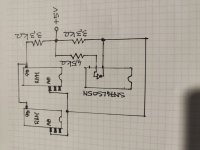
Hi, many thanks for your help. About pins 9 e 15 of the RAM: with a multimeter it seems that are connected to all the ouptut but yesterday I tried to get a schematic from the board and here you can see the vias:

There are other connections on the Schmitt trigger and on the inverter, if it helps I can try to draw all.
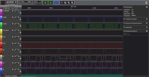
I understood what you are telling me about the CS of the eprom and here you have a new acquisition made with your indication:

here at the start

no CS eprom

At about four seconds from the trigger
There are no outputs from the 4028 and the BCD ouput it's connected to the MC14511BCP BCD to seven segment decoder on the board of the display that normally show the speed of the TT. I remember that sometime ago I replaced the 4028 and the 4511. In the past sometime I saw some segments of the display showing something. About the seven Darlington arrays it seems to me that I've tested it but I'm not sure
There are other connections on the Schmitt trigger and on the inverter, if it helps I can try to draw all.
I understood what you are telling me about the CS of the eprom and here you have a new acquisition made with your indication:
here at the start
no CS eprom
At about four seconds from the trigger
There are no outputs from the 4028 and the BCD ouput it's connected to the MC14511BCP BCD to seven segment decoder on the board of the display that normally show the speed of the TT. I remember that sometime ago I replaced the 4028 and the 4511. In the past sometime I saw some segments of the display showing something. About the seven Darlington arrays it seems to me that I've tested it but I'm not sure
Attachments
- Home
- Member Areas
- Introductions
- Another hello from Italy