ok. but as ph1 & ph2 looks ok, it's not a surprise that 4f0 and 2f0 are ok; those are divider output after the crystal osclillator
Hi sorry I read now you post. Yes I have an old scope, I will try to make some measurements and to draw a diagram. Many thanks
It seems I have a problem with the 5V power supply. 10mS/DIV, 1 VOLT/DIV. In the past I changed the 7805 and the caps, I don't understand, It would be something bad in the power supply line. This is on the VCC of the MC6800P 😢
Is the ground of your scope well connected to the ground of the circuit? the pin14 measurment is really weird.
Is the scope DC coupled? and where is reference (0v ) graduation?
anyway, check input of rectifier bridge to ensure transformer is ok then output of rectifier bridge to see waveform and check if 7805 has enough headroom (>7.5V) to provide a clean 5V.
Caps are the usual suspects (the two blue and the yellow on their left) but it's better to check with a schematic rather than randomly declaring parts faulty...
Yes it's DC coupled, and it seems the ground is well connected, the 0V is in the middle. The caps are brand new It was the first thing I have done some months ago. There are 10.5V at the input pin of the 7805. This is the rectifier bridge output:
10 mS TIME/DIV and .5V VOLTS/DIV
At the rectifier bridge input I've 10.5V and this is rare because I'm quite sure I've measured something like 12,5 sometimes ago. At the 7805 output I've 4,94V
Sorry I'm boring you and yes I agree it would be much better with a schematic
10 mS TIME/DIV and .5V VOLTS/DIV
At the rectifier bridge input I've 10.5V and this is rare because I'm quite sure I've measured something like 12,5 sometimes ago. At the 7805 output I've 4,94V
Sorry I'm boring you and yes I agree it would be much better with a schematic
5V on 7805 output is inconsistent with post #24
With 0V in the middle and DC coupling post#28 could'nt be rectifier out. It looks like it is rectifier out but AC coupled and 0V not in middle but on top. you have .5V ripple which is good.
Could you :
With 0V in the middle and DC coupling post#28 could'nt be rectifier out. It looks like it is rectifier out but AC coupled and 0V not in middle but on top. you have .5V ripple which is good.
Could you :
- connect scope gnd to system gnd
- ensure you have a x1 or a x10 probe
- set scope input coupling to DC
- set scope vertical sensitivity to 1V/div (0.1 if x10 probe)
- set 0V to lowest line of scope screen
- set horizontal to 10 ms/div
- measure : +5V, 6875 pin 12, 6875 pin 14
- Scope connected to system ground
- I have a x1 probe
- I set scope into coupling DC
- 1V/div
- 0V to lowest line
- 10 mS/div
0V at the lowest line
Pin 12 an 14 of 6875.
Thank you
OK, so back to the beginning : it seems there's no issue on VCC and reset.
But what have we seen on post#17 and #18 ?
I think you should retry you measurements but taking in account that you're working with TTL level not 5V CMOS. On the analyser you should be able to choose TTL or to change the treshold for the high level to 2Vmin and if possible for the low level to 0.8V max. Be sure to have proper ground connection between analyser and board.
Thing to check are :
you could also have a look to this : https://pdf1.alldatasheet.fr/datasheet-pdf/download/135447/MOTOROLA/MC6800.html
But what have we seen on post#17 and #18 ?
I think you should retry you measurements but taking in account that you're working with TTL level not 5V CMOS. On the analyser you should be able to choose TTL or to change the treshold for the high level to 2Vmin and if possible for the low level to 0.8V max. Be sure to have proper ground connection between analyser and board.
Thing to check are :
- have a proper reset
- a proper ph1 and ph2
- cpu HALT high (pin2)
- TSC low (pin39)
- activity on all data bus and adress bus lines but also correct TTL levels.
you could also have a look to this : https://pdf1.alldatasheet.fr/datasheet-pdf/download/135447/MOTOROLA/MC6800.html
Last edited:
Hi, thank you. Now, really, I don't know what we have seen in that post but in the past I saw many rare things from this board.
More probably it's my mistake, sorry.
Thank you for the DS it's what I'm reading.
I will check all and post the results
Many thanks as always
More probably it's my mistake, sorry.
Thank you for the DS it's what I'm reading.
I will check all and post the results
Many thanks as always
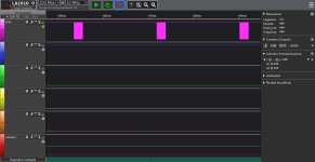
Hello, here you can see the start up of the system. with the analyzer I can't appreciate the non overlapping of the PHI signals I will try to see them on the scope: zooming it's seems the clocks are good.
Some lines of the data buffer
Activity on some lines of the output buffer. It seems always the same byte 🤔 (in the picture not all the byte)
It seems to me that according with your indications something is alive. Am I wrong?
Here I tried to investigate the PIA (EF6821):
The reset signal is ok and when I press the 33 turns key or the 45 turns key that is correctly addressed to the PIA.
I'm reading the DS of the EF6821: I would like to understand what the PIA is sending to the MC6800 and if the MCU is working with these datas.
Attachments
My mistakes of yesterday come out from a bad ground and a bad ground connection between the analyzer and the board. I' haven't realized that is a key feature for good measurements
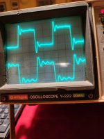
Under you can see phi2, phi1 above. 2V/div, 0,2 microS Time/div. 0V centered where the signal is low, the clock pulse width is at minimum (400 nS) and it seems there are 900 nS total phi1 and phi2 up time but in my opinion those clocks are bad. It seems that the raise and fall time are 40 nS. Reading the DS it seems ok but I haven't experience on those signals
Hi.
That looks better.
First pic on post#36 looks OK, but second with repetitive pattern on data bus with 100ms burst and long (~50ms) period of inactivity is weird.
Third pic , A0- A4 line looks ok with a repetitive pattern but no way to say it's good or bad, this could be a software loop.
Now , we know that 5V is ok, 6875 is ok, and CPU is running or at least try to run. Now it's time to check signal integrity of data bus and address bus, with the scope, not the analyser.
Set your 0, DC coupling, 1V/div, 2 or 5us/div, adjust your probe for under/over shoot with the scope calibrator, check on the CPU all adress lines and all data line and VMA and BA on the CPU, not the 6821. Signal should all have same height, appx 3 to 4.5 V height. take pic of signals that looks bad in comparaison of other and also signal always 0 or 1 or worse : in between.
Post a good quality pic of the board, in order to be able to read the chip references.
Please take note that those are basics tests to do with such a CPU based system. They're intended to detect obvious failure, but going further may be difficult without deeper knowledge, without the schematics, without spare sparts including the eeprom with the software, without a emulator pod,...
Hi, many thanks for the suggestions today I will check all you suggest.
For your last words....yes I agree this is almost an impossible challenge.
For now and sorry if I have bad ideas, but I'm convinced that we are facing a problem with the software (e.g. eprom) or with a bad read of the eprom.
For that and in the aim of not wasting your time I investigate the DS of the TMS2416LS-45 Eprom: if we want to read the eprom the CS and PD/PGM pins are to be low but I always see a clear high signal. On the board these pins are connected and these are the Y7 output of a 74LS138 decoder/multiplexer: according to the true table of the decoder to have a low output on Y7 we need an high on G1 and a low on G2= G2A+G2B. These is what I'm reading on those pins:
G1 pin

G2A

G2B
And here what I'm reading on the CS and PG/PDM of the eprom (the zero is always at the last line of the screen

In my opinion in this condition it's impossible to read the Eprom and for that we have the problem. Am I wasting time? Many thanks as always
For your last words....yes I agree this is almost an impossible challenge.
For now and sorry if I have bad ideas, but I'm convinced that we are facing a problem with the software (e.g. eprom) or with a bad read of the eprom.
For that and in the aim of not wasting your time I investigate the DS of the TMS2416LS-45 Eprom: if we want to read the eprom the CS and PD/PGM pins are to be low but I always see a clear high signal. On the board these pins are connected and these are the Y7 output of a 74LS138 decoder/multiplexer: according to the true table of the decoder to have a low output on Y7 we need an high on G1 and a low on G2= G2A+G2B. These is what I'm reading on those pins:
G1 pin
G2A
G2B
And here what I'm reading on the CS and PG/PDM of the eprom (the zero is always at the last line of the screen
In my opinion in this condition it's impossible to read the Eprom and for that we have the problem. Am I wasting time? Many thanks as always
- Home
- Member Areas
- Introductions
- Another hello from Italy