I want to present you another autobias project. This version we built is designed to work with the Hawksford error correction published in Bob Cordell's book. The principle of operation is based on the patent US4237425 by David A. Spiegel. This principle was elegantly implemented by Shinichi Kamijo at http://www.ne.jp/asahi/evo/amp/J554K2955/index2.htm
In the scheme designed by Mr. Shinichi Kamijo there are several aspects that I thought I needed to change. First of all, I introduced an amplifier stage to reduce the errors caused by the imperfection of the comparators with transistors. Secondly, I even used the resistors from the emitters / sources transistor on the output stage. And finally I replaced the optocoupler with some current source in order not to alter the improvement brought by the error correction
.

.
Despite all these changes to Mr. Shinichi Kamijo's design, the working principle is the same and works very well. I built it in three copies and I am very satisfied with the results. The standby current is constant, it does not depend on the temperature, the amplitude or the frequency of the signal.

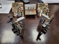
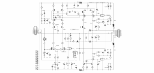
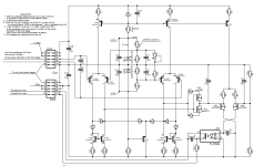
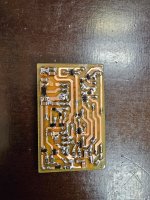
For reasons of easier troubleshooting, the amp is made on interconnectable modules. It consists of front-end, hec, autobias and output stage. I post the Hec to get an overview of how the autobias connects to that Hec at the end (which is generically drawn). The short protection of the output stage is also planted on the Hec plate. There are three pairs of drivers in parallel, considering that at a + -95V power supply with a total current through them of about 75mA, they heat up very well. The interconnection of the plates is done with ribbon cable. The autobias connects directly to the hec board.

A quick search does not show a lot of those devices still available.
Ah, a post with "available" devices
Pretty cool. I need to study it much further. Everytime my model deviated from very conventional, I wound up with increased distortion.
Ah, a post with "available" devices
Pretty cool. I need to study it much further. Everytime my model deviated from very conventional, I wound up with increased distortion.
Might I ask why the high driver current? Don't you only need enough to swamp the gate capacitance?
Maybe I should have pointed out at the beginning that this autobias is for the AB class amplifier. The idle current can be set between 100mA and 200mA per transistor with TR1 and TR2. They are mounted on the same shaft and adjust simultaneously. But they can be replaced with fixed resistors.
To continue, I post the final version (at least at this moment ...) of my front-end. This is Bob Cordell's (very) slightly modified design. I chose Cordell's design for its special stability and very good parameters. The compensation is Tmc. The pair of jfet on the input (smp860) are in the same capsule. Because its maximum source drain voltage is only 20V and because the power supply is + -95V I added a second cascode stage to the entrance to reduce dissipation here, so it does not require radiators. To reduce distortion, the bases of transistors Q3 / Q4 are controlled by a signal identical to the input, so the drain / source voltage of the input jfet is kept fixed, eliminating the Early effect. Several ways can be used to achieve this goal, I chose to obtain this signal from the output signal with the help of resistors R17 and R12. I would also mention the clipping circuit whose threshold is basically determined by the power zenner U1 and U2. In this case they are 75V to achieve a clipping of about 75V-76V. Considering that the hec (Hawksford error correction) stage decreases by about 10V, a clipping of the output signal is cca 65V-66V. The O1 optocoupler provides a signal to the logic block when the cliping comes into action. The current through the input differential is 2mA and through the vas transistors is 10mA . The vas transistors and the current generator require cooling. The coupling with the other stage is made by ribbon cables.
I physically made 6 front-ends (for 3 amps). They all work the same. I specify this to emphasize that the parameters obtained are NOT something isolated, obtained by chance or possibly by mistake (hi). No, the reproducibility is very good. Obviously, with other pcb there may be differences. But the one I made is not a secret, it is available in eagle for those who are interested. To cool the vas transistors, I chose the version from the picture, they will be mounted near the final stage, on the same radiator. That's the concept of the amp. But they can also be mounted on the other side of pcb with independent individual radiators. The pcb is cca 70mm / 92mm.
I physically made 6 front-ends (for 3 amps). They all work the same. I specify this to emphasize that the parameters obtained are NOT something isolated, obtained by chance or possibly by mistake (hi). No, the reproducibility is very good. Obviously, with other pcb there may be differences. But the one I made is not a secret, it is available in eagle for those who are interested. To cool the vas transistors, I chose the version from the picture, they will be mounted near the final stage, on the same radiator. That's the concept of the amp. But they can also be mounted on the other side of pcb with independent individual radiators. The pcb is cca 70mm / 92mm.
Attachments

I'm back with a seventh version of autobias. I do this not because the sixth option would not work well, but because its complexity did not give me peace.
The principle of operation is the same. In short: to determine the quiescent current, the voltages on the emitters (sources) of the transistors (power meters) are used. These voltages are +-35mV (in my case) for a quiescent current value of about 160mA (0.035V / 0.22 ohms=.16A where 0.22 ohms is the value of the resistance in the emitters (sources) of the finals). If a lower value of the idling current is desired, a higher resistance is chosen, so that we have a few tens of millivolts. The small values of these voltages actually represent the challenge in achieving a stable autobias. In the first versions, I tried to use integrated comparators. It was not ok due to the fact that they did not have a fast enough response speed. There followed a variant where I switched to the comparator with transistors but beforehand I amplified the signal to have some reasonable thresholds. This version (in the post above) works ok, but it's a bit complex... So I restarted the design based on a comparator circuit with transistors to process the +-35mV raw signal. This comparator has a very high response speed because of the chosen topology and because (very important!) we did not allow any of the transistors to enter saturation. At the same time, I used paired transistors (two in a capsule) for a better pairing. So, we have two comparators with two inputs each. One compares the positive voltage on the resistor from the emitter (source) above with a positive reference (in my case +35mV) and the other the negative voltage on the other resistor from the emitter (source) with -35mV. It results in four situations. 1. The voltages on the resistors are both lower than the reference. 2. They are both larger in reference mode. 3 and 4. One is bigger and the other is smaller. We are only interested in cases 1 and 2. In the first case the quiescent current is higher than the desired one and in case 2 it is lower. In the first case we must decrease the quiescent current and in the other we must increase it. At the output of the comparators we already have logic signals. To determine the sense in which the quiescent current must be modified, we must use an exclusive-or logic function. Here I made my own contribution by realizing this function with only two mos, one p and the other n. Thus, depending on the output state of the comparators, a 10u capacitor will be charged or discharged. The voltage on this capacitor commands (through a comparator) an optocoupler that will perform the actual adjustment of the quiescent current.
The principle of operation is the same. In short: to determine the quiescent current, the voltages on the emitters (sources) of the transistors (power meters) are used. These voltages are +-35mV (in my case) for a quiescent current value of about 160mA (0.035V / 0.22 ohms=.16A where 0.22 ohms is the value of the resistance in the emitters (sources) of the finals). If a lower value of the idling current is desired, a higher resistance is chosen, so that we have a few tens of millivolts. The small values of these voltages actually represent the challenge in achieving a stable autobias. In the first versions, I tried to use integrated comparators. It was not ok due to the fact that they did not have a fast enough response speed. There followed a variant where I switched to the comparator with transistors but beforehand I amplified the signal to have some reasonable thresholds. This version (in the post above) works ok, but it's a bit complex... So I restarted the design based on a comparator circuit with transistors to process the +-35mV raw signal. This comparator has a very high response speed because of the chosen topology and because (very important!) we did not allow any of the transistors to enter saturation. At the same time, I used paired transistors (two in a capsule) for a better pairing. So, we have two comparators with two inputs each. One compares the positive voltage on the resistor from the emitter (source) above with a positive reference (in my case +35mV) and the other the negative voltage on the other resistor from the emitter (source) with -35mV. It results in four situations. 1. The voltages on the resistors are both lower than the reference. 2. They are both larger in reference mode. 3 and 4. One is bigger and the other is smaller. We are only interested in cases 1 and 2. In the first case the quiescent current is higher than the desired one and in case 2 it is lower. In the first case we must decrease the quiescent current and in the other we must increase it. At the output of the comparators we already have logic signals. To determine the sense in which the quiescent current must be modified, we must use an exclusive-or logic function. Here I made my own contribution by realizing this function with only two mos, one p and the other n. Thus, depending on the output state of the comparators, a 10u capacitor will be charged or discharged. The voltage on this capacitor commands (through a comparator) an optocoupler that will perform the actual adjustment of the quiescent current.
Attachments
Advantages compared to the previous version: smaller size (36mmx56mm), only one trimpot is required to adjust the idle current, much reduced complexity, unpretentious and cheap parts, excellent performance. At the input, I put a 1u capacitor on the branch that forms a low-pass filter with 27 ohm resistors that connect the emitters (sources) of the autobias finals in order not to allow possible high-frequency residues due to the eengine to disturb the autobias. Apart from the 5v1 zenner, all the parts are smds, and I have to admit that it was a bit difficult to make the wiring and mount these smds. It must be emphasized that the heart of this autobias is the two comparators. Due to the high gain, the offset is relatively small, up to +-1mV and stable because they are transistors in the same capsule, so the BE voltages change in the same way (at least theoretically!). But more important than the offset is the response speed. The moments when the voltages on the emitters (sources) are simultaneously higher or lower than the reference are of the order of microseconds and in these extremely short times the actual adjustment is made.
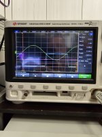
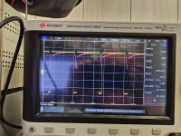
The green oscillogram is the output of the amplifier (out). Yellow and blue are the outputs of the comparators and purple is the voltage on the 10u capacitor C4 on which the correction voltage is stored. The signal frequency is about 1.35 Khz. Oscillogram 2 shows the phase shift between the outputs of the comparators, a phase shift of about 12 uS, during which C4 is charged or discharged depending on the quiescent current value. This is why the comparators have to be very fast. This time of 12 uS decreases with the increase of the working frequency of the amplifier.
Diodes D9 and D10 are not necessary from the point of view of operation. They are needed because the u$1 and u@2 mos have by design protection diodes between DS.
The charging or discharging of C4 is blocked during the time when the outputs of the comparators are simultaneously high or simultaneously low.
Attachments


At the end of my foray into the possibilities of making a relatively cheap (and high-performance!) autobias, I reached option number 8. I'll stop here. I will present one last circuit that seems to be the most stable of all the ones experienced so far. The operating principle is identical to the previous one, but the way of implementation is different. The comparators, the xor circuit and the analog switch are made with logic circuits. Until now, I have kept away from them because they require a 5V power supply, but weighing the advantages, I decided to experiment with one. The indisputable major advantage is the working speed of tens of nanoseconds. As I have already pointed out, the time window in which the quiescent current is measured is of the order of microseconds or tens of microseconds. So the response times of the comparators are needed as low as possible to minimize the errors. Of all the comparison circuits available at Mouser, I opted for the max9012 with a response time below 10 nS and most importantly, without hysteresis. Let's not forget that we are comparing voltages of the order of tens of mV. Together with xor circuit (with Schmitt trigger) and the analog switch, a delay of several tens of nanoseconds is reached. However, this does not allow the determination of the quiescent current at frequencies of tens of kHz or signals of very high amplitude, so a limitation is imposed in the acquisition of the quiescent current signal. I did this with a simple rc filter interleaved at the output of the xor circuit (pin 4) and the control input of the analog switch (pin 6). This filter does not allow the switch to be activated at too high a frequency or at too steep an input voltage. So that the acquisition of the idle current signal is done at idle or only up to a few khz. Otherwise, due to the very high time constants of the integrator that follows the analog switch, the quiescent current is kept constant.
Attachments


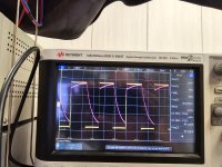
Of all the experienced autobiasurs, this one seems to me to be the simplest, most compact and most stable. The operating principle was attacked head-on, with high-performance parts, with minimal compromises. In the picture with fltru-1 you can see the signal from the input of the analog switch where the frequency is high. It can be seen that the activation signal does not reach the 1.5V threshold required for switching when it reaches filter-2 (lower frequency). The yellow spot is at the xor output (4) and the purple spot is at the analog switch input (6).
Attachments
- Home
- Amplifiers
- Solid State
- Another autobias design...