Being new to the "current mode" switching, I had a look at 4 datasheets, none of the manufacturers (NXP, Fairchild, Ti, Maxim) show a sch that uses what I can recognise as "current mode".
All seem to be showing voltage mode switching !
Am I blind?
All seem to be showing voltage mode switching !
Am I blind?
I've tried to recreate switching characteristics table on page5 of the Ti cd4066b datasheetSWITCHING CHARACTERISTICS
. . . . . . . . . . . . SWITCH INPUT . . . . SWITCH OUTPUT,
VDD. . . . Vis . . . . . Iis (mA) . . . . . . . . Vos (V)
(V) . . . . (V) . –40°C . 25°C . 125°C. . . MIN . . MAX
15 . . . . . 0 . . . . 4 . . . 3.4 . . 2.4 . . . . . . . . . 1.5
15 . . . . 15 . . . .–4 . . –3.4 . . –2.4 . . 13.5
Copyright © 2011, Texas Instruments Incorporated
The last two lines apply when Vdd = 15Vdc
Q1
does this mean there is no requirement to split the supply into +-7.5Vdc?
Vis is the control voltage to turn the switch off or on.
It shows as a nominal 0Vdc for off and 15Vdc for on.
At the extreme right of the table, min and max are given.
Q2
does the 1.5 for max mean that the off control voltage can be anywhere from 0Vdc to 1.5Vdc?
Q3
does the 13.5 for min mean that the on control voltage can be anywhere from 13.5Vdc to 15Vdc?
Being new to the "current mode" switching, I had a look at 4 datasheets, none of the manufacturers (NXP, Fairchild, Ti, Maxim) show a sch that uses what I can recognise as "current mode".
All seem to be showing voltage mode switching !
Am I blind?
Read this informative Analog Devices Tutorial:
http://www.analog.com/static/imported-files/tutorials/MT-088.pdf
figures 23 and 25 should be in your bag of analog design tricks
Those are on page 14 and page 16, but it is worth reading the theory that precedes them.
Regards
If enough folks are interested, I can do a group buy of the ISSL54405ivz (TSSOP16) parts.
Last edited:
google does not recognise the part number. I tried removing ivz, but no finds.If enough folks are interested, I can do a group buy of the ISSL54405ivz (TSSOP16) parts.
Is it known by an alternative?
Sorry but no.Actually, this circuit can handle a ±50V input signal… with the 3.3V powered switch.
Datasheet
http://www.intersil.com/content/dam/Intersil/documents/isl5/isl54405.pdf
clearly states:
And with a higher supply?The inputs can accommodate ground referenced
signals up to 2VRMS while operating from a single 3.3V or 5V DC
supply.
Not higher allowed:
• Single supply operation . . . . . . . . . . . . . . . . . . . . . . . . . 3.3V or 5V
ISL54405
Absolute Maximum Ratings
VDD to GND . . . . . . . . . . . . . . . . . . . . . . . . . . . . . . . . . . . . . . . . . -0.3V to 4.0V
5V_Supply to GND . . . . . . . . . . . . . . . . . . . . . . . . . . . . . . . . . . . -0.3V to 6.0V
Input Voltages
SEL, MUTE, AC/DC, DIR_SEL (Note 6) . . . . . . . . . . -0.3 to ((VDD) + 0.3V)
L1, L2, R1, R2 (Note 6) . . . . . . . . . . . . . . . . . . . . . . -3.1 to ((VDD) + 0.3V)
Output Voltages
R, L (Note 6) . . . . . . . . . . . . . . . . . . . . . . . . . . . . . . . -3.1 to ((VDD) + 0.3V)
You have a problem with the switch, not the resistor.In my test circuit, I use a 10KΩ resistor in series with the switch input and place the switch output at the inverting input of the current to voltage converter stage. So, the switch has 1.9Ω resistance, and the feedback resistor is 3KΩ, so I can put ±50V into the input, limited essentially by the resistor's breakdown ratings
Please read the datasheet which I quoted above.The 3.3V supply of the CMOS switch is not an issue
That's when the switch is ON, then voltage drops across the 10K resistor, producing a current, which will drop a small voltage across the switch internal resistance ... but that's not the point ... any switch must be able to switch OFF ... and there it must stand the full input voltage, because the series resistor does not drop voltage any more.- the switch sees 10mV or so of signal with a 50V input
That is not true when the switch is OFF ... which is an expected function of any switch.... Again… I'm switching _current_ and all of the voltage has been dropped by a factor of 5000 by the input resistor ahead of the switch.
You have a signal current only when switch is ON; but when OFF it must stand full voltage.The inverting current to voltage amplifier that follows the switch converts the signal current back into a voltage and all is well again.
Agree that using TWO switches has better attenuation than using just ONE 🙂Off leakage also gets nice since you can shunt the input signal current to ground when the switch is off - it's a DPDT switch, so when it's on, you can wire it to feed signal current into the virtual ground, and when it's off, send the signal current to ground.
I'd love to check the feed through pulses during the short time when both switches are OFF during transition
, the grounding switch has not yet closed and the series so called "current" one has to stand the full 50V 😱The ISL54405 features a soft-switch feature
I guess my terminology is misleading - The switch is a DPDT, so the signal is connected through the resistors to either of two outputs, one a VE summing stage (what I call "on") and another, signal ground (what I call "off). When the switch is "off", the signal is shunted to signal ground, so you get the same drop across the input 10K resistor. It's a DPDT, and I do this for off isolation, to keep the input impedance constant, and also to preserve the input voltage tolerance. There is still 10mV across the switch in all conditions, since the output of the switch is either ground or virtual ground.
Transitions are definitely interesting, and I have not yet tested those. The 'break before make' time may kill me, or the switch, but we shall see.
Transitions are definitely interesting, and I have not yet tested those. The 'break before make' time may kill me, or the switch, but we shall see.
Last edited:
Instantaneous signal voltage must always reside between Vdd and Vss, among which the maximum difference possible is 15V DC.I've tried to recreate switching characteristics table on page5 of the Ti cd4066b datasheet
The last two lines apply when Vdd = 15Vdc
Q1
does this mean there is no requirement to split the supply into +-7.5Vdc?
Whether you use a symmetrical supply, a positive one or a negative one is not important as far as signal swings between them.
Yes.Vis is the control voltage to turn the switch off or on.
It shows as a nominal 0Vdc for off and 15Vdc for on.
At the extreme right of the table, min and max are given.
Q2
does the 1.5 for max mean that the off control voltage can be anywhere from 0Vdc to 1.5Vdc?
Yes.Q3
does the 13.5 for min mean that the on control voltage can be anywhere from 13.5Vdc to 15Vdc?
Edit: to be more precise, that control voltage is relative to Vss , no matter where it stands (which depending on circuit chosen may lie anywhere between Gnd and -15V) .
Last edited:
Thanks JMF and MMcG for current mode switching tutorials in post 11 & 14. RCA was sold off about the time they invented CD4016 and CD4066. so no I have no app notes or seminar time on analog switches. I bought 100 DPDT telephone relays to do some analog switching inside my H100 organ, but 3PDT CMOS switches are so much lighter and more compact. I'm doing some analog tone generation to supplement the sine waves I already have available- trangle waves and half waves. They have to switch in before the mixer transformer, which is current mode. I proved in experiments on hydrophones and TI digital field systems decades ago,double throw relays make a big pop into an amplifier input when they switch over.
Last edited:
Hello
I've been using the SSM2402 audio analog switches for a long time with excellent results but I just discovered it's been discontinued since few years.
Any suggestion for an equivalent, Analog Devices or other?
I need to apply on ±18 V or less supply, below 100 ohms ON resistance, great isoltaion resistance, very low distortion, 2 x spdt function, pin DIP version, Rhos or not...
Thanks!
Luke
LDR's when biased on so their signal resistance is 50-100 ohms make excellent switches
for audio signals. see attached datasheet, You need to observe to limit LED current to 16ma or lower.
Attachments
That's what worries me.The 'break before make' time may kill me, or the switch, but we shall see.
Nor burning anything, power involved is minuscule, but I fear narrow but loud transients passing through.
Might sound like "not sure they're there" clicks, and counter intuitively, increasing filtering (delayin switching more) might actually increase them, contrary to expected.
There is an external switching time delay capacitor, CAP_SS which might be tweaked to optimize balance switching click vs. possible high signal feedthrough , weird thing is that switching OFF takes 50 nS, switching ON takes 1M times longer 58 mS 😱
While we would need both to happen at roughly the same time, for flawless switching.
Weird.
Although M Mc G valuable experiment might give us a nice surprise: maybe the switch stands more than expected 🙂
Or maybe the switch may be used without the switching delay cap (or with a minuscule one ).
Only testing knows the answer .
Fact is, we are being forced more and more towards SMT, specially on all new devices.
Which is great for factories and the end consumer, not so much for home experimentors 🙁
The way they spec the on and off times is pretty confusing. There is the NO/NC switching, controlled by the SEL pin, and there's the MUTE switching. From what I've decoded, if you never use mute, then the CAP_SS controls the changeover speed from one output to another, driven by the SEL pin. However going into mute is very rapid, and turning on from mute follows the CAP_SS speed.
I've got a pulse generator on the SEL input now and I can definitely see a slow ramp on, but my pulse generator (HP 8082A) is too fast compared to the CAP_SS and it seems to be doing something odd (not fully cycling on or off, sometimes doing the ramp and sometimes not), so I have to put in a smaller CAP_SS and keep poking at it. This could also simply be an artifact of my scope triggering!
I've got the scope synced to the pulse generator, so I will also look for any spikes or other BS. Hoping that they aren't there, but more work needs to be done. 🙂
It's probably already been said, but I think the main reason some analog switches need to switch current rather than voltage is primarily because their power supply limits are smaller than typical voltage swings of audio signals.
I used several AD analog switches many years ago, switching voltages not current, run off a 15 volt supply, and had no problems. I first measured the output impedance of the switches to get an idea of their ability to generate distortion, and then scaled the circuit values so this wouldn't be an issue.
I used several AD analog switches many years ago, switching voltages not current, run off a 15 volt supply, and had no problems. I first measured the output impedance of the switches to get an idea of their ability to generate distortion, and then scaled the circuit values so this wouldn't be an issue.
google does not recognise the part number. I tried removing ivz, but no finds.
Is it known by an alternative?
My error ISL54405IVZ (too many essses)
250 parts are $1.60 ea at Newark Elec.
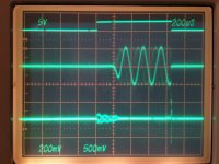
Here's a scope photo of the ISL54405 using a 470pF CAP_SS value. The top trace is the pulse generator, which triggers all of the traces in ALT mode. The second trace is the output of the I/V stage, whose gain is set by the 10KΩ input (pre-switch) resistor and a 3.01KΩ feedback resistor with a 1VRMS 5KHz input. The third (bottom) trace is the input to the ISL54405, after the 10KΩ input resistor.
In the second trace, you can see the soft start function working as predicted. However, you can also see that the output goes to "off" extremely abruptly, essentially as they say the switches operate when going into MUTE mode.
The third trace show a very narrow glitch as the switch is turned off (if my understanding of the triggering setup is correct). This amplitude is equal to the input signal amplitude (1.4V peak), which shows that the input node goes high impedance for a very short time as the switch is turned off. The start of the waveform, just as the 'on' pulse starts is pretty odd though, and I don't know what to make of it. It looks like a signal is turned on immediately, then faded down at the CAP_SS rate, like the fadeout I was hoping for in the main output.
So, there are more tests to do, and I have to make sure that my setup and the scope triggering are what I think they are. But indeed, the switch has a very brief time (less than 10µs?) when it goes high impedance, So, the input signal voltage does have limits imposed by the low power supply voltage. However, in normal operation, the voltage at the switch input is very low, so this peak could be clamped with diodes to protect the switch without touching the signal in normal operation.
Regards,
Attachments
"current mode" is indeed a clever way to use a cmos switch.
some designers have even included a switch in the feedback loop of the inverting amplifier following the switch to compensate for the on resistance variation. works well, although you do lose a switch. combine this scheme with the baxandall tone control and feedback volume control and then one more inverter to get the polarity "correct" (all using inverting op amp stages so low cm related distortion) and you'll be in opamp heaven, if that floats your boat.
🙂
mlloyd1
How about using PhotoMOS relays?
Panasonic makes a pair of components called AQY221R2S and AQY221N2S.
One with 0.8Ω Ron and 13pF output capacitance, and the other with 9.5Ω Ron and 1pF output capacitance.
I know that you get zero crossing distortion in a triac based SSR (if I'm not mistaken), but is it also something that plague the PhotoMOS relays?
There is no zero crossing distortion with photo relays. A larger version using discrete FET's and a photovoltaic couplers has proved very successful as a speaker relay. In fact there is a large thread on the forum on those. Post #61 shows the circuit.
http://www.diyaudio.com/forums/solid-state/191449-output-relays-4.html#post2620430
Those Panasonics would be to costly compared to other options, around £5 GPB even in 250+ quantity.
http://www.diyaudio.com/forums/solid-state/191449-output-relays-4.html#post2620430
Those Panasonics would be to costly compared to other options, around £5 GPB even in 250+ quantity.
- Status
- Not open for further replies.
- Home
- Source & Line
- Analog Line Level
- Analog switches