Not at all.
The biggest variable will be the cost of the chassis, some people are able to knock one out with some big heatsinks from the scrapyard and some sheet metal, and others are completely dependent on buying something from the store. (I fall into the later camp, sadly)
But that said, a budget of $500-700 will have you completely covered. Maybe a bit less if you are able to dive into parts you have laying around. More if you want it to look like a million bucks.
Hi, thank's for sharing your build. I am tempted to build a venerable Pass amp but I am a little concerned by the power consumption of theses amps. Do you have some real world measurements (idle, 20, 50, 100% volume) ?
Greetings
Greetings
between 150 and 180W per stereo amp ...... mostly depending how much you bias it
being A class , it'll soak it all the time
being A class , it'll soak it all the time
I am a little concerned by the power consumption of theses amps. Do you have some real world measurements (idle, 20, 50, 100% volume) ?
As ZM said, It's a class-A amp, so the current draw from the mains is constant regardless of output. Approx 150-180W, as he says.
i see. thanks. Are there any Pass builds that use less current with the same sound quality or are the high use of energy and the high sound quality linked ?
Sent from my phone using Tapatalk
Sent from my phone using Tapatalk
Real Class-A is hot and burns a lot of standing current. There's no getting away from that.
It's also why they sound so much better than everything else...
It's also why they sound so much better than everything else...
When setting the bias on my F5 I used tape to hold my DMM k-type thermoprobes to the heat sink and FETs. It occurred to me that the k-type probes are probably just a thermistor on the end of a wire. I know there are a lot of different types of thermistors but I was wondering if it's possible to just clip onto the F5 thermistors to get an on FET reading or will the DMM throw off the temp compensation circuit and vice versa the temp compensation circuit would throw off the reading of the DMM? Depending on the thermistor couldn't we have a table of resistance values to map to temperatures?
1) not everyone has temp on their dmm or a separate IR temp gauge.
2) wouldn't it be a more direct reading of the FET than through a heat sink? Putting tape over the thermoprobe tip to adhere it could help retain heat and throw off the reading.
3) could be a check point for the thermistors and give visibility into what's happening in the heat compensation circuit.
4) isn't it easier to clip a couple of leads to the thermistors than placing a thermoprobe by tape? With tape I worry whether it's touching or if there's a slight minuscule gap, also, slight movements with the cables could move the probe tip.
I can't see any other way than to express any change of voltage across NTC except as percentage or ratio ......
however crude procedure it seems , palm technique combined with DVM for Iq and DVM for offset - is pretty much effective
however crude procedure it seems , palm technique combined with DVM for Iq and DVM for offset - is pretty much effective
Thanks ZM for the reply. Yeah, I just thought it might be cool to check the thermistors instead but I guess palm to heatsink is practical enough. My curiosity still has me wondering how much of a difference there is between heatsink temp and the thermistors.
I also recall asking last year about placing the thermistors touching the FET casing vs the drain leg because I had read on the FET spec sheets that the drain leg gives the highest temp and I noticed the First Watt pics show the thermistors touching the drain. But it's more practical to just have them touch the casing instead with no chance of shorting the FET.
I guess that covers all of my thermistor questions, for now. Haha thanks guys.
The faster the Thermal path from the heat generator to the heat sensor, the more quickly and with less overshoot can the sensor react to the change in heat in the generator.
For that reason many have looked at fitting output stage sensors closer to the heat generator. Sanken and OnSemi have a range of devices with the sensor inside the output device package. Cordell and others have written up how much this improves accuracy of the sensor correction strategy. Self looked at mounting the sensor on top of the metal To3 device.
The Thermistor of an F5 is just such a sensor.
It should, for best correction performance, be inside the output stage devices.
The next best is glued to the Drain lead at the point where it exits the package. If this gives too much correction for changes in heating, then the solution is NOT to move the Thermistor to a longer delayed thermal path.
The proper solution is to change the tempco ratios so that the correction matches the change.
To date I cannot recall anyone suggesting changes to the resistor:thermistor resistance ratios to change the tempco.
Pass did bring out a modified topology of where the Thermistor fits into the feedback circuit. This may have been prompted by looking for a better tempco to more accurately sense the changes and make the necessary correction.
Last edited:
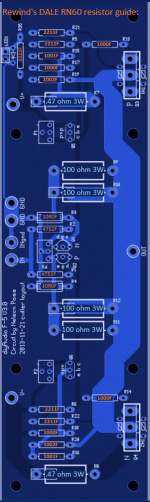
For the lazy f-5 builder:
Cvillers F-5 v3.0 pcb board is nice, but differs from the Cviller v2.0 BOM in the DiyAudio.com shop. I lost a night of happy amp building because of this "update", so I spent the next night going through the resistors and flexing my skills in MS paint.
The guide is based on the non-turbo F-5 amplifier schematic in the Nelson Pass F-5 Turbo article, using Dale RN60 resistors. The .zip file contains an Excel file with the schematic and a list of resistors, if you want to double check. You should!
I used this site to search values: http://www.datasheets360.com/part/detail/rn-55-d-1001-f/-746750307682916945
Attachments
Last edited:
The stuffing of the Cviller f-5 v.3.0 boards continues.
It turns out a n00b can turn something very simple into something very complicated.
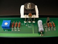
Like fitting trimpots. I wanted to be true to the original design by Nelson Pass by using the same type of flat trimpots with the three pins in a triangle pattern (see attached picture of the factory version of the F-5). This illustrated guide uses a different type of standing trimpots with the three pins in a straight line.
In the Bourns datasheets the pins are named "1", "2" and "3". When looking at examples of the cviller boards the pins were reversed! With a triangle shaped trimpot I have difficulties reversing it, because the pins are to short to bend that far.
Solution, I think, is that I will need to turn the knob of the trimpots in whatever direction - clockwise or counterclockwise - as I end up with. RIGHT? A confirmation from a trimpot expert would be nice.
Also, when fitting P3 with these flat trimpots, the trimpot overlaps the holes for the LS74 and the LSK170 JFETS. Solution - bend the pins like an L and move the trimpot 3 mm away.
It turns out a n00b can turn something very simple into something very complicated.
Like fitting trimpots. I wanted to be true to the original design by Nelson Pass by using the same type of flat trimpots with the three pins in a triangle pattern (see attached picture of the factory version of the F-5). This illustrated guide uses a different type of standing trimpots with the three pins in a straight line.
In the Bourns datasheets the pins are named "1", "2" and "3". When looking at examples of the cviller boards the pins were reversed! With a triangle shaped trimpot I have difficulties reversing it, because the pins are to short to bend that far.
Solution, I think, is that I will need to turn the knob of the trimpots in whatever direction - clockwise or counterclockwise - as I end up with. RIGHT? A confirmation from a trimpot expert would be nice.
Also, when fitting P3 with these flat trimpots, the trimpot overlaps the holes for the LS74 and the LSK170 JFETS. Solution - bend the pins like an L and move the trimpot 3 mm away.
Attachments
Last edited:
The single in line (sil) pin trimpot can be inserted in either orientation.
I, but maybe not many others, prefer a clockwise rotation to have the effect of increasing the result, eg. clockwise for increased volume, or increased bias current, or increased etc....
The sil pot can give this clockwise increasing result, or the opposite. And by reorienting it can give what the operator requires (remembers ?).
The staggered pin pot can only be inserted in one orientation.
The layout designer determines whether it gives clockwise = increasing, or anti-clockwise = increasing.
But I suspect most layout designers don't consider this at all.
I saw one PCB that had two staggered pin trimpots. One gave an increase with clockwise and the other gave a decease with clockwise and no label/s to explain the rotation. How stupid was that?
The PCB shown in post757 allows either a sil or staggered pin multi-turn trimpot for all three locations.
None of those locations allows a "flat" style ¾turn trimpot to be fitted that I am familiar with.
Last edited:
With flat I meant a 3386F-1-502LF Bourns Inc. | 3386F-502LF-ND | DigiKey
instead of a standing 3296Y-1-502LF Bourns Inc. | 3296Y-502LF-ND | DigiKey
I did not understand what a "flat" style ¾turn trimpot is and why it does not fit. Did you mean something like this? http://www.texim-europe.com/product/3006P-1-103-BRN
instead of a standing 3296Y-1-502LF Bourns Inc. | 3296Y-502LF-ND | DigiKey
I did not understand what a "flat" style ¾turn trimpot is and why it does not fit. Did you mean something like this? http://www.texim-europe.com/product/3006P-1-103-BRN
Last edited:
- Home
- Amplifiers
- Pass Labs
- An illustrated guide to building an F5