Yes, RCA connectors are abysmal. Use BNC!
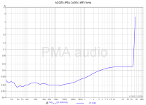
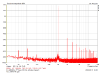
All audio amps should have an input filter to reduce RF ingress, block DC, and limit bandwidth - it can also sometimes prevent slew-rate limiting in the rest of the amp. Testing without that filter is harsher and may catch instabilities that don't show up easily with the filter in place.
All audio amps should have an input filter to reduce RF ingress, block DC, and limit bandwidth - it can also sometimes prevent slew-rate limiting in the rest of the amp. Testing without that filter is harsher and may catch instabilities that don't show up easily with the filter in place.
Likewise, balanced signals on TRS connectors is not the most clever solution, too.
In my problem amp for example, unplugging the input is a sure recipe to trigger some oscillation that otherwise is difficult to provoke.
Even if the amplifier has proper connectors, you never know what kind of cables or adaptors somebody may connect.
In my problem amp for example, unplugging the input is a sure recipe to trigger some oscillation that otherwise is difficult to provoke.
Even if the amplifier has proper connectors, you never know what kind of cables or adaptors somebody may connect.
+1One might ask why am I testing such things like large signal square response. The answer is easy - the amplifier must be designed to survive worst case scenario and to keep speakers safe.
I always test the step response of an amp both with a small signal (so a few volt peak-to-peak on the output) and large signal (say 80% of the full output swing) for that reason. Then drive the amp to clipping with a sine wave and see how it recovers.
I'm not completely shocked that the simulation doesn't match reality perfectly when it comes to stability. I bet the capacitance of the various devices is somewhat poorly modelled. In addition, all the layout parasitics and power supply parasitics are not modelled.
Tom
Until simulators can model oscillators correctly, they will always be deficient in modelling gain circuits. This is why specialist oscillator software exists. LTspice is a basic level simulator.
I like integrated amplifiers because the gain is usually not set to maximum. 🙂
I agree with PMA's sentiments that the amount of feedback required to obtain ultra-low THD is at odds with more important design criteria. IMO, the two amplifiers use high and silly high amounts of feedback. I come from the Leach "Low TIM" school of design where 25dB of loop gain is typical.
Ed
I agree with PMA's sentiments that the amount of feedback required to obtain ultra-low THD is at odds with more important design criteria. IMO, the two amplifiers use high and silly high amounts of feedback. I come from the Leach "Low TIM" school of design where 25dB of loop gain is typical.
Ed
Last edited:
Those structures with complicated frequency compensation (amp #2) like TPC or 3-pole also tend to have quite violent step response with shape dependent on amplitude, when they are driven from impulse generator with short rising edge. The amp is losing FB control and different pole time constants play the game. This may be fixed, for input signal, by quite aggressive input RC filter, but it then affects HF audio band roll-off and phase.
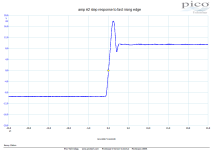
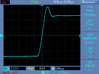
We do not want this behaviour. Aperiodic, level invariant step response is highly appreciated.


We do not want this behaviour. Aperiodic, level invariant step response is highly appreciated.
Large signal steps are useful for stress-testing an amp, but it never happens with an audio bandwidth signal in modern amps which have plenty of slew-rate headroom. The shape of the large signal step response is nothing to worry about - see Figure 17 in the OPA1612 datasheet, not pretty, but that chip manages unity-gain stability, 0.000015% THD and 27V/µs slew rate (way above any normal audio signal).
The only situation I see issues with is feeding an analog synth output direct into an amplifier that lacks an input roofing filter - those synth circuits can produce very wideband signals and steps.
The only situation I see issues with is feeding an analog synth output direct into an amplifier that lacks an input roofing filter - those synth circuits can produce very wideband signals and steps.
This is how the step response changes with output level. In this case, simulations fit with reality quite well.The amp is losing FB control and different pole time constants play the game.
This is definitely something we do not want to happen. But the harmonic distortion is low, so who cares? 😉
Something to consider with these tests is how/when the amp oscillates. If there is no oscillation with no signal or a low level dignal, but the amp shows oscillation at signal peaks that are close to the rails, or just large signal, then a probable cause is that device parameters are being shifted dynamically by the large voltages involved. Cob for example will be higher when Vce is at minimum and conversely, lower at maximum Vce. The Bowes [sp?] test was conceived to look for just such eventualities. This behavior is another one of those parasitic problems that usually won’t get solved by tweaking the loop compensation. Another thing to watch out for is the VAS to ground capacitance through the VAS heat sink tab if the device being used has one.
Simulators don’t do clipping very well - you almost never see the rail sticking and oscillatory recovery you would see in an amp with bad overhang. While the amp is clipping, it’s running with the full open loop gain and the VAS devices are often badly overdriven, then taking a few us before the loop regains control when the source signal moves away from overdrive. As the loop is reasserting itself, overshoot or burst oscillation will manifest for a few us. Baker clamps or VAS transistor current limiting can help mitigate this. Again, this is another class of parasitic instability that cannot usually addressed with loop compensation.
Simulators don’t do clipping very well - you almost never see the rail sticking and oscillatory recovery you would see in an amp with bad overhang. While the amp is clipping, it’s running with the full open loop gain and the VAS devices are often badly overdriven, then taking a few us before the loop regains control when the source signal moves away from overdrive. As the loop is reasserting itself, overshoot or burst oscillation will manifest for a few us. Baker clamps or VAS transistor current limiting can help mitigate this. Again, this is another class of parasitic instability that cannot usually addressed with loop compensation.
Last edited:
My last amp is a three pole compensated blameless. Despite the fact that it has crazy parameters in the simulator, it is stable even in real world.
Small signal AC analysis
ULGF 3 MHz
PM 64 deg
GM 17 dB
LG1k 112 dB
LG10k 110 dB
LG20k 88 dB
CLG 29 dB
Large signal transient analysis
The square wave is stable up to 4R ll 10nF without an output coil. This is enough to use a small 0.1uH coil to isolate the amp output. Instead of a normal coil, I use 35cm long twisted wire terminated by zobel placed on the output terminals of the chassis.
First zobel on the amp pcb -> 35 cm twisted wire -> second zobel on the terminals or on the SSR pcb.
That screen looks like it is slew rate limited.While presented analysis and conclusions are excellent, it must be pointed out that response into 150 nF/4.7 Ω, as seen above, is very likely not sign of approaching low phase margin, rather LCR resonant response on fast enough stimulus. There is typical amplitude fall like in a resonant circuit with low Q.
I’ll try to elaborate.
First let’s check response of very fast power amplifier with low dV/dt signal. Capacitor is connected, as is in OP example, with test leads (120 cm total wire length) and internal amplifier wiring is only 30 cm total (both wires). Signal rise time is 3 us into 47 nF||4.5 Ω. We can see that there is practically clean response.
View attachment 1252289
There's no indication of a well controlled rise/fall time, just straight edges.
Jan
No. It is an amplifier with <300 ns rise time, so signal generator was limited to 3 us rise time to be somewhat comparable with Sinclair amplifier example. It has perfectly symmetric rise/fall times with square wave signal up to the clipping point.That screen looks like it is slew rate limited.
There's no indication of a well controlled rise/fall time, just straight edges.
My point was that, while there is always a difference between simulation and real circuit (for all well-known reasons), presented example with 150 nF load didn’t represent without doubt point of compromised stability. Due test setup with long test leads, it is more likely RLC resonance. It may be that Sinclair amplifier is absolutely stable with that capacitive load, as was in the simulation.
Again, I wanted to point that during test with capacitive load, we should carefully examine to not mix RLC resonance with instability. Capacitor should be at amplifier’s binding posts for that test.
It’s important to note there will always be RLC ringing in an amp - even in non feedback amps. It’s just a consequence of driving a fast rise time signal into the resonant circuit formed by the cable and any associated capacitance and another reason why a damped output coupling inductor is a good idea - especially for feedback amps.
For stability testing, a resistive load must be used initially and the square wave response checked for fidelity before any capacitive load drive is tested.
Here is a useful rule of thumb for determining the signal BW given the rise time:-

For stability testing, a resistive load must be used initially and the square wave response checked for fidelity before any capacitive load drive is tested.
Here is a useful rule of thumb for determining the signal BW given the rise time:-
Last edited:
Depends where it is measured. I measure DF at amplifier output terminals, however I measure the step response at the PCB point before the output coil (if the coil is used), to know exactly what is the amp doing. Of course with 1m wires and measurement at the load there MUST be a RLC ringing, but it is unimportant re amp stability.It’s important to note there will always be RLC ringing in an amp - even in non feedback amps. I
Yes, it has nothing to do with stability, that’s why it has to be removed as a confounder during initial testing with a resistive load.Depends where it is measured. I measure DF at amplifier output terminals, however I measure the step response at the PCB point before the output coil (if the coil is used), to know exactly what is the amp doing. Of course with 1m wires and measurement at the load there MUST be a RLC ringing, but it is unimportant re amp stability.
Well, something is slew limiting. Look at post # 37, that's a nice collection of RC-risetime limited waves. The one you showed earlier has straight edges and no RC risetimes. It's a classic example of a slew limited waveform.No. It is an amplifier with <300 ns rise time, so signal generator was limited to 3 us rise time to be somewhat comparable with Sinclair amplifier example.
I don't know where it comes from but it is easily recognized.
Jan
Yes, it has nothing to do with stability stability, that’s why it has to be removed as a confounder during initial testing with a resistive load.Depends where it is measured. I measure DF at amplifier output terminals, however I measure the step response at the PCB point before the output coil (if the coil is used), to know exactly what is the amp doing. Of course with 1m wires and measurement at the load there MUST be a RLC ringing, but it is unimportant re amp stability.
Yes, as said, it was adjusted at the signal generator. Not caused by amplifier.Well, something is slew limiting.
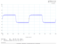
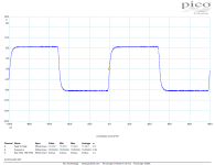
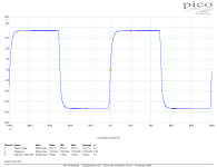
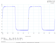
Here are unlimited responses at 100 kHz. Amplifier has +/- 17 V supply.
4 Vpp/8Ω
28 Vpp/8Ω
- Home
- Design & Build
- Electronic Design
- Amplifiers - Feedback/Loopgain stability simulated vs. real world
