...haven't been here for quite some time.)
Hi Matthias, I will study your circuit before I reply in detail but nice to see you back with more ideas.🙂
Best wishes
David
Hi David, thanks in advance.Hi Matthias, I will study your circuit before I reply in detail but nice to see you back with more ideas.🙂
Kind regards,
Matthias
Cont. of post #80: Principle of compensation
In order to introduce the compensation scheme, I will first go from inner to outer loops, adding one loop at a time. This will not yet reflect the full picture, since in reality all signals from the different loops overlay. Nevertheless, it provides first good insight, and it follows the intuitive approach taken in Johan Huijsing's great op amp book, see post #1. The "real" analysis will follow in the next post.
To start with the TMC (transitional Miller compensation) loop, the global feedback resistor R13 is connected to node 'z' (for ensuring operating point), and the "lower ends" of C7 and R53 are grounded. Thus, all loops enclosing the TMC loop are disabled. The probe is inserted between amp output and R6:
probe-tmc.png

This gives the bode plot for the TMC loop with embedded active VAS loop which in turn will be probed later:
bode-tmc.png

Now we close the TMC loop and probe between amp output and the intermediate loop via R53; the other loops are still disabled:
probe-cf.png

This gives the feedback in the intermediate loop that resembles a bit a current-feedback loop and encloses the active VAS and TMC loops:
bode-cf.png

Next we close the current-feedback loop via R53 and probe the (modified) nested Miller compensation loop via C7:
bode-nmc.png

Finally, all inner loops are closed, and the probe is placed between amp output and R13:
bode-global.png

The gain of the global loop and thus the whole amp exhibit second-order behaviour. Otherwise, the input stage distortion would dominate the distortion of the complete circuit. Removing the pole created by C7 and R22 leads to first-order behaviour around the input stage. With a more linear input stage or when accepting the distortion dominance of the input, one could therefore probably achieve a square wave response without overshoot. For the necessity of R21 see e.g. post #1 and especially post #16; the same accounts for the total of (R55+R60||R53).
(This is perhaps the most significant drawback of the nested feedback loop approach: the input stage only sees a small part of the feedback around the output stage. On the other hand, it is an advantage, if one does not like higher-order behaviour of the global feedback loop and thus the whole circuit. Whether the nested loop scheme provides some benefit in terms of robustness of the whole amp, is still unclear. I have contacted an expert in control theory, and will study a bit their advanced methods to evaluate stability. In principle, this also touches the comparison between amps with TMC and two-pole compensation schemes.)
So far, we have a first conceptual picture of the overall compensation scheme. As Dave Zan pointed out several times, this is not enough to correctly judge stability. One has to probe the internal loops and of course also the total feedback around the output stage in normal operation of the whole circuit. I will discuss the results in the next post.
Matthias
[[
Here is the missing square-wave response. As I only now discovered, it is spoiled. It looks fine, with overshoot due to two-pole global loop, till about 2V into 4R. Then an asymmetry between positive and negative overshoot develops. Here is the 1V square wave into 4R, probed directly at the output, still before the inductor.
square.png

]]
In order to introduce the compensation scheme, I will first go from inner to outer loops, adding one loop at a time. This will not yet reflect the full picture, since in reality all signals from the different loops overlay. Nevertheless, it provides first good insight, and it follows the intuitive approach taken in Johan Huijsing's great op amp book, see post #1. The "real" analysis will follow in the next post.
To start with the TMC (transitional Miller compensation) loop, the global feedback resistor R13 is connected to node 'z' (for ensuring operating point), and the "lower ends" of C7 and R53 are grounded. Thus, all loops enclosing the TMC loop are disabled. The probe is inserted between amp output and R6:
probe-tmc.png
This gives the bode plot for the TMC loop with embedded active VAS loop which in turn will be probed later:
bode-tmc.png
Now we close the TMC loop and probe between amp output and the intermediate loop via R53; the other loops are still disabled:
probe-cf.png
This gives the feedback in the intermediate loop that resembles a bit a current-feedback loop and encloses the active VAS and TMC loops:
bode-cf.png
Next we close the current-feedback loop via R53 and probe the (modified) nested Miller compensation loop via C7:
bode-nmc.png
Finally, all inner loops are closed, and the probe is placed between amp output and R13:
bode-global.png
The gain of the global loop and thus the whole amp exhibit second-order behaviour. Otherwise, the input stage distortion would dominate the distortion of the complete circuit. Removing the pole created by C7 and R22 leads to first-order behaviour around the input stage. With a more linear input stage or when accepting the distortion dominance of the input, one could therefore probably achieve a square wave response without overshoot. For the necessity of R21 see e.g. post #1 and especially post #16; the same accounts for the total of (R55+R60||R53).
(This is perhaps the most significant drawback of the nested feedback loop approach: the input stage only sees a small part of the feedback around the output stage. On the other hand, it is an advantage, if one does not like higher-order behaviour of the global feedback loop and thus the whole circuit. Whether the nested loop scheme provides some benefit in terms of robustness of the whole amp, is still unclear. I have contacted an expert in control theory, and will study a bit their advanced methods to evaluate stability. In principle, this also touches the comparison between amps with TMC and two-pole compensation schemes.)
So far, we have a first conceptual picture of the overall compensation scheme. As Dave Zan pointed out several times, this is not enough to correctly judge stability. One has to probe the internal loops and of course also the total feedback around the output stage in normal operation of the whole circuit. I will discuss the results in the next post.
Matthias
[[
Here is the missing square-wave response. As I only now discovered, it is spoiled. It looks fine, with overshoot due to two-pole global loop, till about 2V into 4R. Then an asymmetry between positive and negative overshoot develops. Here is the 1V square wave into 4R, probed directly at the output, still before the inductor.
square.png
]]
Cont. of post #83: Detailed loop probes
[[
Worried about the bad square-wave response from the last post. Will disable all elements for stage overdrive protection and also use first-order feedback around input stage. With the input filter 1k||470p, i.e. tau=0.5us, a 10V square wave asks for around 40V/us. A drive of 5mA from the intermediate stage into a VAS with around 50pF suggests a capability of 100V/us.
But somewhat proud of not exactly optimal, but simple and fast new loop through R53 and the trick with L2.
Pardon for simply continuing.
]]
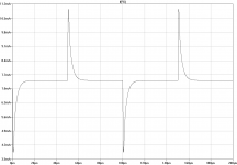
I'd like to start with the most interesting and not yet fully understood point, the total feedback around the output stage. These are measurement and result:

Figure probe-ops

Figure bode-ops
One may still increase the simulated gain margin to 20dB with a small C+R parallel to R6, say 10p+470R. This also shifts the 180-degree frequency to higher values, but leaves ULGF almost unaltered. For the other loops, including VAS loop, this seems to have no influence.
In the discussion following the results from post #73, we agreed that the interaction between different feedback paths has to be watched, see e.g. posts #74 to #76 from Paul and David. This seems still true for me, although the phase reversal and gain notch in post #73 happen at high absolute gain values, so that oscillation may not occur.
In the current design, the notch has "morphed somehow" into a change of gain slope. It is, at least at first sight, less worrying. If one places an isolation buffer (E block with unity gain) between node 'y' and the "lower end" of R6, then one gets the following plot:

Figure bode-ops-iso
Due to some overload, I had to stop thinking about this issue after post #79, but surely it is again on the list. The chair now has four legs, which probably is not better than three when asking for stability ;-).
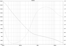
Now the "simpler" things. Feedback seen by the input stage transistor Q7 equals the global NFB loop from figure 'bode-global' in post #83. The total feedback input seen by the intermediate stage is the sum of signals through the global NFB via R13 and the path via C7. Probing circuit for the base of Q1 and bode plot are:

Figure probe-Q1

Figure bode-Q1
In order to probe the inner loop formed by Q1 and Q9, I have placed the probe directly in front of the base of Q9. The result is:

Figure bode-Q9
The output capacities of Q2 and Q3 in the input stage have noticeable positive impact on the phase margin for Q9, as they provide a high-frequency path from the base of Q1 to ground. To see the loop in some isolation, one can again connect R13 to node 'z' and ground C7:

Figure probe-Q9-iso
The result is (the same for very high frequencies as in the previous bode plot, since the surrounding loops have much lower ULGF):

Figure bode-Q9-iso
At lower frequencies, the loop gain is dominated by R25 and C10, higher frequencies are controlled by R28 and C14, very high frequencies by the transistor role-offs. The path with (R28+R27) and C14 is the counterpart for the pole from R22 and C7 which creates the second-order feedback seen by the input stage; it corresponds to R41 and C10 in the design from post #45.
The path via R25 and C10 ensures that the loop gain in the loop of Q1 and Q9 does not fall too much with lower frequencies. Otherwise, the input impedance of the intermediate stage would drop too much. When removing R25 and C10, one really gets slightly higher distortion figures. Perhaps, this is in some contrast to textbook whisdom.
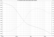
The total NFB signal across the common-base operated Q8 stems from the paths via R13, C7, and now additionally R53. Placing the probe into the emitter of Q8 yields:

Figure bode-Q8
The small inductor L2, that improves margins in the outer stages, is clearly affordable. L2 really does impair the margins at Q8, since the part of high-frequency signal, that is "shifted to the front stages", does not completely return through these stages; they are too slow.
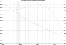
Finally, here is the gain inside of the VAS loop formed by Q13, Q14, C1, and C8 (overlayed by the less wideband surrounding feedback loops). A probe in the base of Q13 gives:

Figure bode-vas
The wheel to turn here is of course R18. But the current status seems acceptable.
Altogether, the stability margins of the circuit look reasonable for my understanding.
Gain margins are always around 20dB in direction of higher frequencies. Going towards lower frequencies from the ULGF, the gain is almost always less than 20dB at the next frequency with phase allowing oscillation. Since the circuit behaviour here is much better controlled and mainly determined by passive components, this should be tolerable.
Worst phase margin of around 40 degrees is seen in the total loop around the output stage, see figure 'bode-ops' above. Again, it is mainly determined by passive components and therefore should be quite reliable. Additionally one may argue with the general observation made in the thread 'Phase margins in higher-order / nested loops' from December 2013, which unfortunately is not yet fully understood. I hope, further study of control theory can bring some progress here.
I still have to check different difficult loads. The most demanding version is probably purely capacitive, leading to resonances with the output inductor L1 at varying frequencies, only damped by the parallel resistor R19.
Matthias
[[
Worried about the bad square-wave response from the last post. Will disable all elements for stage overdrive protection and also use first-order feedback around input stage. With the input filter 1k||470p, i.e. tau=0.5us, a 10V square wave asks for around 40V/us. A drive of 5mA from the intermediate stage into a VAS with around 50pF suggests a capability of 100V/us.
But somewhat proud of not exactly optimal, but simple and fast new loop through R53 and the trick with L2.
Pardon for simply continuing.
]]
I'd like to start with the most interesting and not yet fully understood point, the total feedback around the output stage. These are measurement and result:
Figure probe-ops
Figure bode-ops
One may still increase the simulated gain margin to 20dB with a small C+R parallel to R6, say 10p+470R. This also shifts the 180-degree frequency to higher values, but leaves ULGF almost unaltered. For the other loops, including VAS loop, this seems to have no influence.
In the discussion following the results from post #73, we agreed that the interaction between different feedback paths has to be watched, see e.g. posts #74 to #76 from Paul and David. This seems still true for me, although the phase reversal and gain notch in post #73 happen at high absolute gain values, so that oscillation may not occur.
In the current design, the notch has "morphed somehow" into a change of gain slope. It is, at least at first sight, less worrying. If one places an isolation buffer (E block with unity gain) between node 'y' and the "lower end" of R6, then one gets the following plot:
Figure bode-ops-iso
Due to some overload, I had to stop thinking about this issue after post #79, but surely it is again on the list. The chair now has four legs, which probably is not better than three when asking for stability ;-).
Now the "simpler" things. Feedback seen by the input stage transistor Q7 equals the global NFB loop from figure 'bode-global' in post #83. The total feedback input seen by the intermediate stage is the sum of signals through the global NFB via R13 and the path via C7. Probing circuit for the base of Q1 and bode plot are:
Figure probe-Q1
Figure bode-Q1
In order to probe the inner loop formed by Q1 and Q9, I have placed the probe directly in front of the base of Q9. The result is:
Figure bode-Q9
The output capacities of Q2 and Q3 in the input stage have noticeable positive impact on the phase margin for Q9, as they provide a high-frequency path from the base of Q1 to ground. To see the loop in some isolation, one can again connect R13 to node 'z' and ground C7:
Figure probe-Q9-iso
The result is (the same for very high frequencies as in the previous bode plot, since the surrounding loops have much lower ULGF):
Figure bode-Q9-iso
At lower frequencies, the loop gain is dominated by R25 and C10, higher frequencies are controlled by R28 and C14, very high frequencies by the transistor role-offs. The path with (R28+R27) and C14 is the counterpart for the pole from R22 and C7 which creates the second-order feedback seen by the input stage; it corresponds to R41 and C10 in the design from post #45.
The path via R25 and C10 ensures that the loop gain in the loop of Q1 and Q9 does not fall too much with lower frequencies. Otherwise, the input impedance of the intermediate stage would drop too much. When removing R25 and C10, one really gets slightly higher distortion figures. Perhaps, this is in some contrast to textbook whisdom.
The total NFB signal across the common-base operated Q8 stems from the paths via R13, C7, and now additionally R53. Placing the probe into the emitter of Q8 yields:
Figure bode-Q8
The small inductor L2, that improves margins in the outer stages, is clearly affordable. L2 really does impair the margins at Q8, since the part of high-frequency signal, that is "shifted to the front stages", does not completely return through these stages; they are too slow.
Finally, here is the gain inside of the VAS loop formed by Q13, Q14, C1, and C8 (overlayed by the less wideband surrounding feedback loops). A probe in the base of Q13 gives:
Figure bode-vas
The wheel to turn here is of course R18. But the current status seems acceptable.
Altogether, the stability margins of the circuit look reasonable for my understanding.
Gain margins are always around 20dB in direction of higher frequencies. Going towards lower frequencies from the ULGF, the gain is almost always less than 20dB at the next frequency with phase allowing oscillation. Since the circuit behaviour here is much better controlled and mainly determined by passive components, this should be tolerable.
Worst phase margin of around 40 degrees is seen in the total loop around the output stage, see figure 'bode-ops' above. Again, it is mainly determined by passive components and therefore should be quite reliable. Additionally one may argue with the general observation made in the thread 'Phase margins in higher-order / nested loops' from December 2013, which unfortunately is not yet fully understood. I hope, further study of control theory can bring some progress here.
I still have to check different difficult loads. The most demanding version is probably purely capacitive, leading to resonances with the output inductor L1 at varying frequencies, only damped by the parallel resistor R19.
Matthias
Last edited:
Phase margins
Just (and thus too late) re-checked results and noted, that in fact almost all phase margins are only around 40 degrees, except for global loop around input stage.
Thin ice ...
Matthias
Just (and thus too late) re-checked results and noted, that in fact almost all phase margins are only around 40 degrees, except for global loop around input stage.
Thin ice ...
Matthias
Square waves
Argh. I'm not working in the car industry. So the amplifier will need a switch to toggle between music mode and test signal mode.
The problem from the last posts is appearently cured by a combination of the following things.
1) Increase of VAS current; 5mA seem good for audio-frequency sine waves.
This might call for other Q14 and Q15 types, e.g. 2SA1381 / 2SC3503.
2) Increase of quiescent current in intermediate stage.
This is easily done.
3) Reduction of current corner frequency 320kHz in input filter.
80 kHz are probably acceptable.
4) Less or even no second-order feedback around input stage (increase of C7).
This is a bit subtle. First, it really avoids overshoot and thus unsymmetric overshoot, an obvious sign of problems. But even if the square wave looks OK, one may of course have problems in internal stages, cured only by 1) to 3). Secondly, an increase of C7 shifts the feedback away from the input stage, but it remains available around the output stage. This also means that the behaviour e.g. in figure 'bode-nmc' of post #83 becomes second-order. Now it is still unclear, whether one can find a network instead of C7, R22, R21, and C9 that produces first-order behaviour for the first stage, if the enclosed loop is of second order. The simple trick from post #16 works for first order. Just removing C7 and R22 results in a strange bode plot with "steps" for the input stage.
One solution would be to also remove the zero created by R28 and C14. Then, one would have enough free gain to push further the NFB via R53, so that the loop gain increase in figure 'bode-cf' of post #83 extended further to lower frequencies. This would somewhat compensate the loss of gain around the ouput stage due to cancelation of the R28/C14 zero.
Finally, this all depends on a better input stage.
But perhaps this is the direction eventually to go.
Here is a square wave 5V into 4R before the output inductor. I have changed currents in VAS and intermediate stage to around 10mA and input filter to 160kHz. Loop characteristics are unchanged, but protection elements R56 and D2 are disabled. (R58 at basis of driver Q17 helps the simulator in finding the initial operating point.)

Figure square-schem

Figure square-out
This plot shows the driving current via R5 from the intermediate stage. One sees that the circuit is near the limit, since again the current approaches zero.

Figure square-R5
The input stage is working hard, collector current of Q7. The developping asymmetry is already visible.

Figure square-Q7
To be complete, finally the sine wave spectra (still taken in the original circuit) at 2kHz and 200Hz, 10V into 4R.

Figure spectrum-2k

Figure spectrum-200
These too will never ever be possible in the real amp. But thanks to great books like the ones from Robert Cordell and Douglas Self one can try to avoid at least the simplest mistakes in building the beast. The ear will judge.
Matthias
Argh. I'm not working in the car industry. So the amplifier will need a switch to toggle between music mode and test signal mode.
The problem from the last posts is appearently cured by a combination of the following things.
1) Increase of VAS current; 5mA seem good for audio-frequency sine waves.
This might call for other Q14 and Q15 types, e.g. 2SA1381 / 2SC3503.
2) Increase of quiescent current in intermediate stage.
This is easily done.
3) Reduction of current corner frequency 320kHz in input filter.
80 kHz are probably acceptable.
4) Less or even no second-order feedback around input stage (increase of C7).
This is a bit subtle. First, it really avoids overshoot and thus unsymmetric overshoot, an obvious sign of problems. But even if the square wave looks OK, one may of course have problems in internal stages, cured only by 1) to 3). Secondly, an increase of C7 shifts the feedback away from the input stage, but it remains available around the output stage. This also means that the behaviour e.g. in figure 'bode-nmc' of post #83 becomes second-order. Now it is still unclear, whether one can find a network instead of C7, R22, R21, and C9 that produces first-order behaviour for the first stage, if the enclosed loop is of second order. The simple trick from post #16 works for first order. Just removing C7 and R22 results in a strange bode plot with "steps" for the input stage.
One solution would be to also remove the zero created by R28 and C14. Then, one would have enough free gain to push further the NFB via R53, so that the loop gain increase in figure 'bode-cf' of post #83 extended further to lower frequencies. This would somewhat compensate the loss of gain around the ouput stage due to cancelation of the R28/C14 zero.
Finally, this all depends on a better input stage.
But perhaps this is the direction eventually to go.
Here is a square wave 5V into 4R before the output inductor. I have changed currents in VAS and intermediate stage to around 10mA and input filter to 160kHz. Loop characteristics are unchanged, but protection elements R56 and D2 are disabled. (R58 at basis of driver Q17 helps the simulator in finding the initial operating point.)
Figure square-schem
Figure square-out
This plot shows the driving current via R5 from the intermediate stage. One sees that the circuit is near the limit, since again the current approaches zero.
Figure square-R5
The input stage is working hard, collector current of Q7. The developping asymmetry is already visible.
Figure square-Q7
To be complete, finally the sine wave spectra (still taken in the original circuit) at 2kHz and 200Hz, 10V into 4R.
Figure spectrum-2k
Figure spectrum-200
These too will never ever be possible in the real amp. But thanks to great books like the ones from Robert Cordell and Douglas Self one can try to avoid at least the simplest mistakes in building the beast. The ear will judge.
Matthias
Last edited:
Acknowledgement
There is still a lot to figure out, and finally the beast may stay unborn or prove to be a technical or musical disaster.
Although I haven't been here for quite some time, I do not want to miss the opportunity to thank all of you who helped me over the time to develop the current design. It was and hopefully will continue to be a pleasure to share, discuss and develop ideas, correct mistakes, or complain about the wheather with you.
In the danger of forgetting somebody (my apologies in advance), I would like to name
Cheers and See you,
Matthias
There is still a lot to figure out, and finally the beast may stay unborn or prove to be a technical or musical disaster.
Although I haven't been here for quite some time, I do not want to miss the opportunity to thank all of you who helped me over the time to develop the current design. It was and hopefully will continue to be a pleasure to share, discuss and develop ideas, correct mistakes, or complain about the wheather with you.
In the danger of forgetting somebody (my apologies in advance), I would like to name
dadod, DaveZan, jcx, kgrlee, mcd99.
Thank you.
Cheers and See you,
Matthias
...not yet fully understood point, the total feedback around the output...
Sorry to take a while to respond but I really don't understand this plot.
I have seen similar, "inexplicable" plots in the past.
I believe it is caused partly by the way LTspice determines the 0 reference to plot phase.
I have no idea what that way is, but it seems it can lead to bizarre results when there is feed-forward and/or Non Minimum Phase behavior.
Feed-forward usually means alternate paths thru a circuit and this often causes NMP behavior so I don't know which is the actual cause.
It may be possible to sort this out with TRAN simulations of pulses, they would eliminate the problem that phase is somewhat arbitrarily defined.
I don't feel confident to comment on the finer details when I don't understand even the simpler case of the total feedback plot.
On the positive side, since our last discussion I have had a minor epiphany and now understand much better how to optimize 3 section amplifiers.
So I am even more convinced that 3 sections are all one needs😉
Optimized 3 section amps tend not to have this kind of mysterious phase plot.
In fact I consider it an indication that there is some complexity that could be simplified.
So I had pushed this problem to the back of my mind.
Thank you for the chance to learn more, your amplifiers are always fun intellectual puzzles!
If anyone knows about this Spice issue then I would love to see an explanation or reference.
Best wishes
David
Hi David,
thank you for the comments. I will need some time to fully understand your remarks and to gain sufficient distance from the "binge writing" during the last days.
Kind regards,
Matthias
thank you for the comments. I will need some time to fully understand your remarks and to gain sufficient distance from the "binge writing" during the last days.
Kind regards,
Matthias
I still need to think this over some more but I have had one small idea.
It is known that the Tian analysis is not quite strictly complete.
To be specific, it does not handle "null transmission" very well.
Usually this makes very little practical difference in a conventional amplifier, not sufficient to justify the use of a more accurate but more complicated technique.
I suspect the multiple gain sections in your amplifier may expose the incompleteness of Tian.
If so then a Middlebrook analysis should be clearer.
I started a thread on this a while back, easy to find if you are interested.
Also, it may be worth an inquiry on the LTspice Yahoo group.
Best wishes
David
Undesirable loop in circuit
Hi David,
thank you for the additional thoughts.
I think, there is at least some truth in the Tian probe result. Firstly, with Middlebrook probe, the problem "vanishs". Result is like in post #84 with isolation buffer for the TMC loop, figure 'bode-ops-iso'.
Secondly, as mentioned in post #77 discussing the previous design, there is indeed an active loop bypassing the output stage. Through the TMC resistor R6, the VAS drives into the feedback path via front stages, working against the output impedance of the ouptut stage, which is open-loop in the range 0.1 to 0.2R. Below the strange knee around 45kHz in figure 'bode-ops' of post #84, the simulated gain of this loop exceeds unity. Luckily, this now somehow does not lead anymore to a worrying gain peak with sharp phase reversal.
Since the discussion of the previous design it is puzzling me that this "stray loop" apparently does not impair distortion performance. All additional loops I added over time to the circuit resulted in the expected improvements.
(Maybe, I expected too little. As I understand and respect, this is one of your points, David ;-)
Placing an isolation buffer between amp output and R6 does not change distortions, although the above reasoning would suggest that. One can e.g. deliberately underbias the output stage and observe harmonics of a 5kHz sine wave. The harmonics will be mainly created by the output stage and do not change with isolation buffer for R6. If the knee were real and also affected the NFB linearisation mechanism, then the larger loop gain around output stage should bring better results with buffer.
Altogether, there is something going on in the loops I do not really understand. This seems to be independent of possible problems with the Tian probe.
Can anybody else comment on these issues? Is a kind of bootstrapping mechanism working here?
Kind regards,
Matthias
Hi David,
Kind regards,
Matthias
nice to read that. Have you already described it somewhere? From Jan Didden's abstract, I'd conclude that it is not yet in your last Linear Audio paper?On the positive side, since our last discussion I have had a minor epiphany and now understand much better how to optimize 3 section amplifiers.
As I have tried to say in post #91, we share this general impression. You also see it from a more abstract perspective, something I would like to learn a bit more, too. Maybe, it will be a result of my planned studies in control theory that hopefully can lead to better understanding of nested loops.... In fact I consider it an indication that there is some complexity that could be simplified ...
You are welcome!Thank you for the chance to learn more, your amplifiers are always fun intellectual puzzles!
Can you please give a further clue? Cannot find this thread on the Tian probe issue.I started a thread on this a while back, easy to find if you are interested.
Kind regards,
Matthias
...nice to read that. Have you already described it somewhere? From Jan Didden's abstract, I'd conclude that it is not yet in your last Linear Audio paper?
I was finally able to mathematically optimize the nested loops
It is intended it to be the conclusion of my Linear Audio papers but I haven't finished the write up yet.
Been distracted by other jobs but I am almost ready to return to it.
Can you please give a further clue? Cannot find this thread on the Tian probe issue.
Thread is >Here<
I just had a quick review of it, there's not much about the Middlebrook probe but there is some discussion of nested loops and the phase anomaly.
Best wishes
David
Last edited:
Wish you good progress! I really look forward to seeing some results backed up by fundamental arguments.I was finally able to mathematically optimize the nested loops
It is intended it to be the conclusion of my Linear Audio papers but I haven't finished the write up yet.
Thank you for the time.Thread is >Here<
I just had a quick review of it, there's not much about the Middlebrook probe but there is some discussion of nested loops and the phase anomaly.
Matthias
Last edited:
Square waves
I was still thinking about the surprising problem with square-wave response. Now, a majour issue came to my mind, and it is confirmed by simulation.
The current swing delivered through R5 during transients (figure 'square-R5' in post #86) largely goes into the NFB network via L2. Thus, only a fraction is fed into the VAS via R54 and Q8.
The short reasoning from beginning of post #84 therefore is wrong. The quiescent current of intermediate stage is not fully available for charging the VAS Miller capacity when slewing. It is only about one tenth.
Still do like nested loops; they are challenging.
Matthias
Hi Matthias,
Do you have LTSpice files for download? From the pictures your spice style is very
sophisticated, even more parameterized than mine 🙂
I like to simulate such complex systems with ideal npn and pnp transistors.
It is easier to add step for step nonideal behaviour to the transistors and see what the
effect on stability is.
Greetings,
Udo
Hi Udo,... and see what the effect on stability is ...
I have sent a PM.
Kind regards,
Matthias
Merry Christmas!
Hi Everybody,
as seen in post #85, post #91, and post #95, there are some minor and majour problems. They have to be fixed, or I have to courageously ignore them before ordering and soldering. The right balance of, e.g., slew rate (power bandwidth) and distortion performance is unclear.
I will return to this thread next year. Looking at the view figures, there is at least some interest in what this crazy person is simulating there.
I wish you all a Merry Christmas,
Matthias
Last edited:
Looking at the view figures, there is at least some interest in what this crazy person is simulating there.
I wish you all a Marry Christmas,
Matthias
Hi Matthias,
Yes there is always hidden interest in threads. I for one have been lurking on this one. Lack of free time prevents involvement though.
Looking forward to you building this. 🙂
Merry Christmas to you too!
Paul
Version with better slew rate
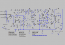
For the intermediate loop in the design from post #80, I have found a solution with acceptable slew rate. Additionally, now a JFET input stage is used.
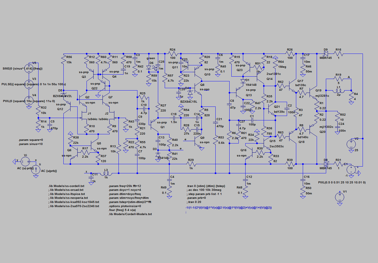
Figure schematic
The loop via R53 and C21 in the new circuit does not contain the kind of shunt gain shaping with C21 and (R55+R60||R53) in the version from post #80. This shunt shaping grounded more current swing than necessary. Still, the new feedback loop takes away a substantial portion of the current swing delivered by the intermediate stage; otherwise it could not contribute to the NFB budget. Nevertheless, a reasonable square-wave response is possible, see below.
The gain shaping zero from C21 and (R55+R60||R53) in the old circuit is now created by C14 and R54 in the intermediate stage. R28 and C15 supress loop gain peaking. The simple intermediate stage with Q1 and Q9 can produce the necessary second-order characteristic with low distortion, if Q9 has good current gain and early voltage.
Until now, I could not find a replacement for the L2 trick in post #80. A small lead compensation capacitor parallel to R5, for instance, impairs stability margins in the loop formed by Q1 and Q9. One can use a small capacitor between input-stage output and emitter of Q8 as high-frequency feedforward path, but this does only bring very little. So, all gain margins now are a bit lower, but always above 15dB. Phase margins and ULGFs in all loops are similar to those in post #83 and post #84.
Here are the loop gain around input stage (global NFB) and the total NFB seen by the output stage. The latter is probed both with Tian and Middlebrook probes, see the problem in post #91.
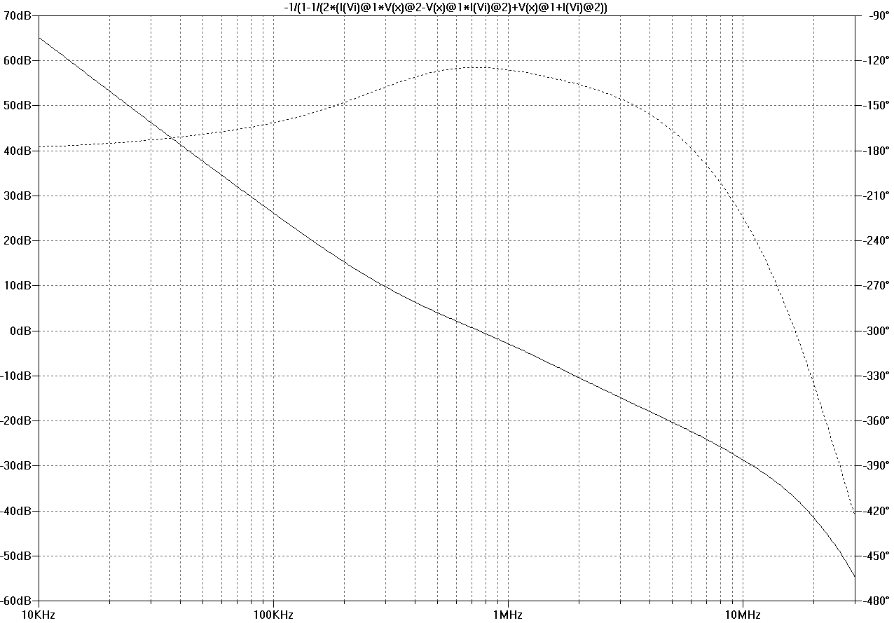
Figure bode-global

Figure bode-ops-tian

Figure bode-ops-middlebrook
Inspired by the thread "Overunity transistors", I have played with different transistor types and models. The types 'ss-npn' and 'ss-pnp' are e.g. BC550C/BC560C from Bob Cordell or KSC1845/KSA992 from ONsemi, depending on the active lib file. Robustness against these small signal types and models, and also against driver / output types, is quite good. The bode plots above use Bob's BC5xx and other models. My impression is that these always give the worst results.
Simulated THD20 at 100kHz bandwidth is below 1ppm, here are the spectra for 10V and 1V into 4R. (At 2kHz, simulation results approach the ppb region, see end of post #86.)
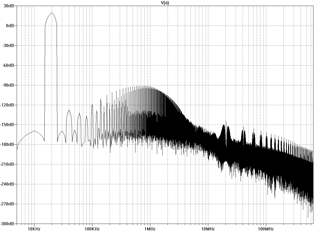
Figure THD20-10V
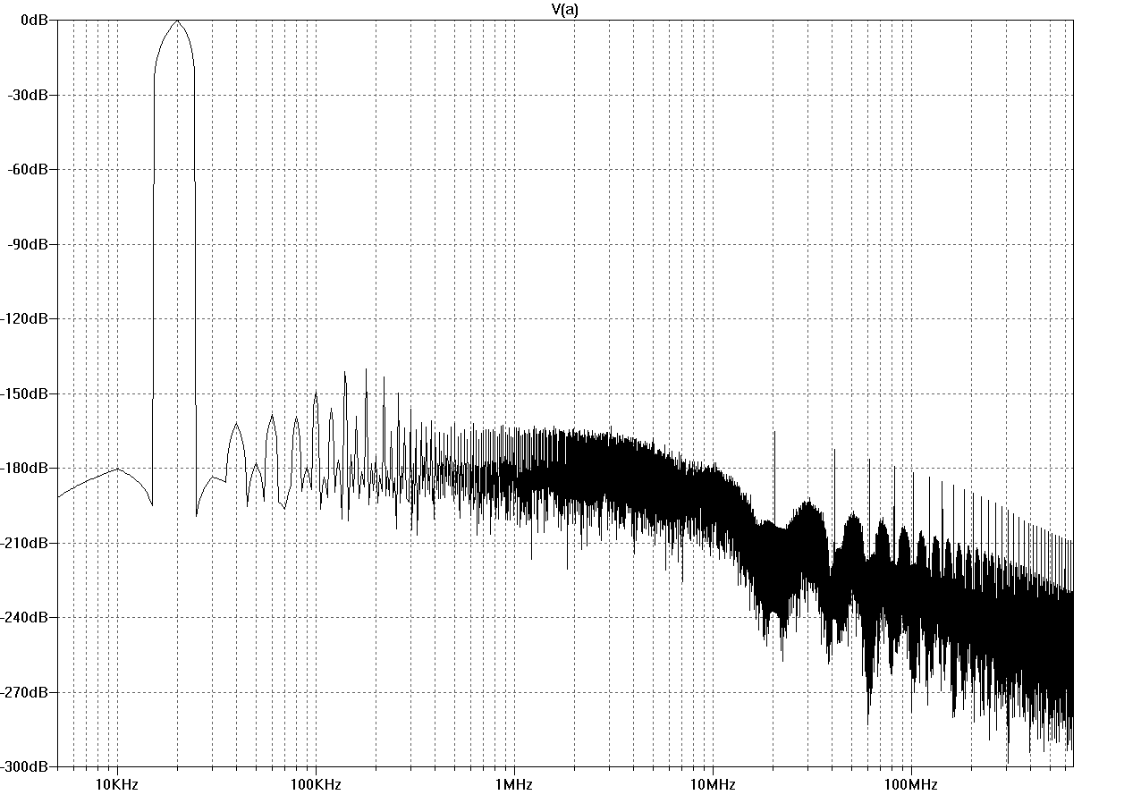
Figure THD20-1V
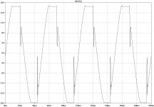
Finally, square-wave response 10V into 4R with 320kHz input filter, probed before the output inductor. Voltage swings with 20V/us during edges.
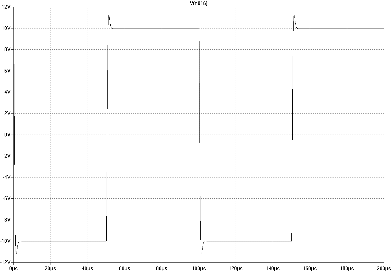
Figure square-out
A closer view shows that the falling edge is slightly disturbed. It becomes clean with larger load resistance. Base charge removal from output transistors is probably not fast enough with 25mA and 50mA as driver and output quiescent currents.
Here are current in R5 (output of intermediate stage) and drain current of input stage JFET J2, load is 4R. The small "distortion" in square-R5 at 100us+ vanishs with higher load.

Figure square-R5
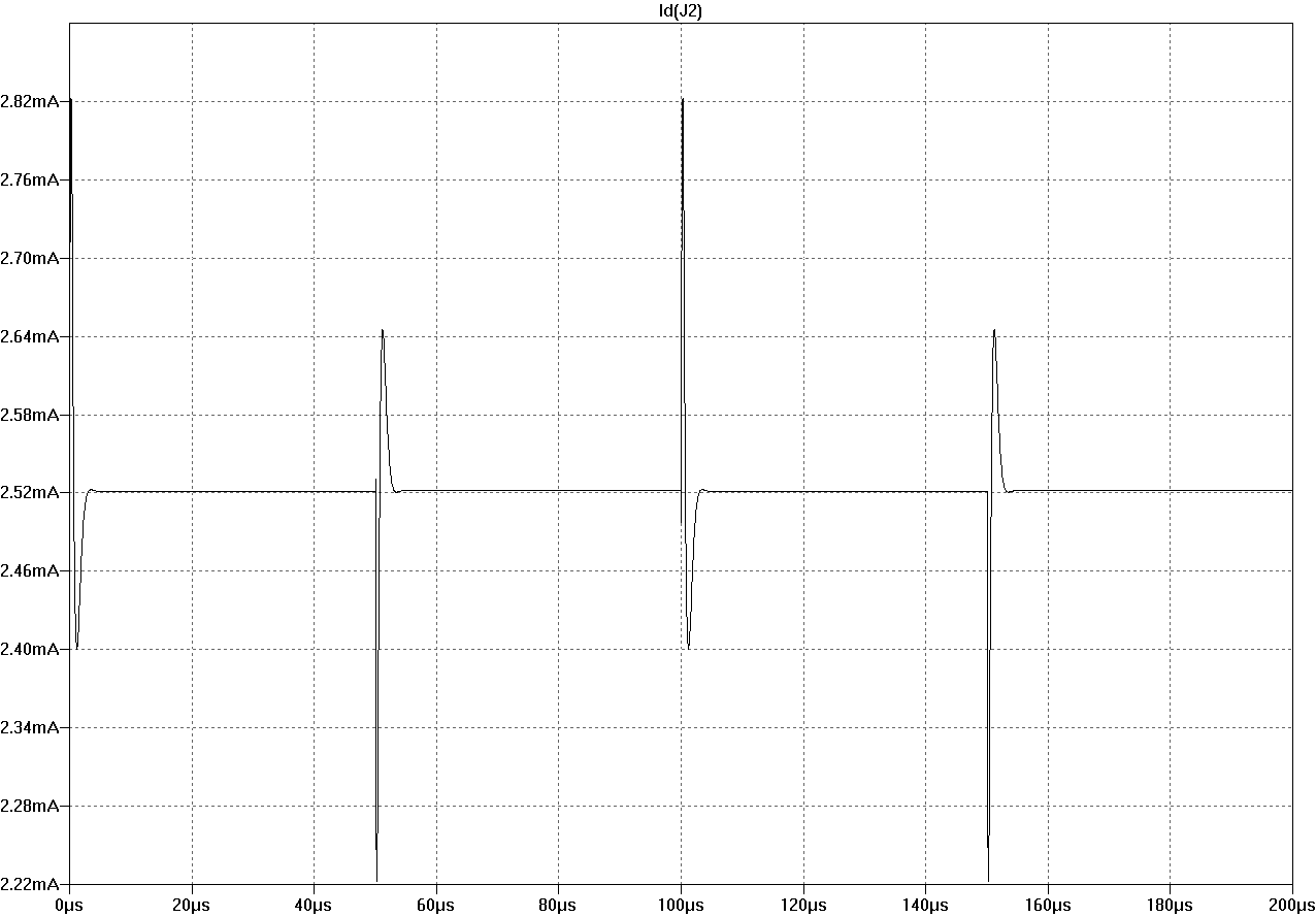
Figure square-J2
Clipping behaviour became bad, but the circuit remains stable, and my music hopefully won't clip it.
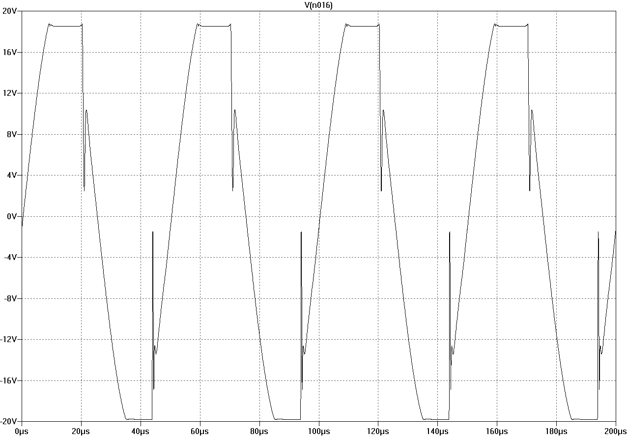
Figure clipping
Although the dissipation due to VAS quiescent current of 7mA would still allow to use BC546B/BC556B, I now have taken 2SC3503/2SA1381. When playing with the internal VAS loop gain, I found that the high base spreading resistance included in Bob's BC5xx models (also corresponding to the ONsemi datasheet for BC550/BC560) does reduce stability margins in VAS and also other loops. I do not know, whether all transistors from the BC5xx family have this large base spreading resistance. Perhaps, one could also use 2N4501.
For the other general problem from post #91, I have a first idea. Will need some more time.
Matthias
For the intermediate loop in the design from post #80, I have found a solution with acceptable slew rate. Additionally, now a JFET input stage is used.
Figure schematic
The loop via R53 and C21 in the new circuit does not contain the kind of shunt gain shaping with C21 and (R55+R60||R53) in the version from post #80. This shunt shaping grounded more current swing than necessary. Still, the new feedback loop takes away a substantial portion of the current swing delivered by the intermediate stage; otherwise it could not contribute to the NFB budget. Nevertheless, a reasonable square-wave response is possible, see below.
The gain shaping zero from C21 and (R55+R60||R53) in the old circuit is now created by C14 and R54 in the intermediate stage. R28 and C15 supress loop gain peaking. The simple intermediate stage with Q1 and Q9 can produce the necessary second-order characteristic with low distortion, if Q9 has good current gain and early voltage.
Until now, I could not find a replacement for the L2 trick in post #80. A small lead compensation capacitor parallel to R5, for instance, impairs stability margins in the loop formed by Q1 and Q9. One can use a small capacitor between input-stage output and emitter of Q8 as high-frequency feedforward path, but this does only bring very little. So, all gain margins now are a bit lower, but always above 15dB. Phase margins and ULGFs in all loops are similar to those in post #83 and post #84.
Here are the loop gain around input stage (global NFB) and the total NFB seen by the output stage. The latter is probed both with Tian and Middlebrook probes, see the problem in post #91.
Figure bode-global
Figure bode-ops-tian
Figure bode-ops-middlebrook
Inspired by the thread "Overunity transistors", I have played with different transistor types and models. The types 'ss-npn' and 'ss-pnp' are e.g. BC550C/BC560C from Bob Cordell or KSC1845/KSA992 from ONsemi, depending on the active lib file. Robustness against these small signal types and models, and also against driver / output types, is quite good. The bode plots above use Bob's BC5xx and other models. My impression is that these always give the worst results.
Simulated THD20 at 100kHz bandwidth is below 1ppm, here are the spectra for 10V and 1V into 4R. (At 2kHz, simulation results approach the ppb region, see end of post #86.)
Figure THD20-10V
Figure THD20-1V
Finally, square-wave response 10V into 4R with 320kHz input filter, probed before the output inductor. Voltage swings with 20V/us during edges.
Figure square-out
A closer view shows that the falling edge is slightly disturbed. It becomes clean with larger load resistance. Base charge removal from output transistors is probably not fast enough with 25mA and 50mA as driver and output quiescent currents.
Here are current in R5 (output of intermediate stage) and drain current of input stage JFET J2, load is 4R. The small "distortion" in square-R5 at 100us+ vanishs with higher load.
Figure square-R5
Figure square-J2
Clipping behaviour became bad, but the circuit remains stable, and my music hopefully won't clip it.
Figure clipping
Although the dissipation due to VAS quiescent current of 7mA would still allow to use BC546B/BC556B, I now have taken 2SC3503/2SA1381. When playing with the internal VAS loop gain, I found that the high base spreading resistance included in Bob's BC5xx models (also corresponding to the ONsemi datasheet for BC550/BC560) does reduce stability margins in VAS and also other loops. I do not know, whether all transistors from the BC5xx family have this large base spreading resistance. Perhaps, one could also use 2N4501.
For the other general problem from post #91, I have a first idea. Will need some more time.
Matthias
Attachments
-
 square-J2.png15.3 KB · Views: 277
 -
 square-R5.png15.9 KB · Views: 274
 -
 square-out.png14.5 KB · Views: 289
 -
 THD20-1V.png24.2 KB · Views: 290
 -
 THD20-10V.png24.5 KB · Views: 300
 -
 bode-ops-middlebrook.png24.9 KB · Views: 278
 -
 bode-ops-tian.png26.5 KB · Views: 297
 -
 bode-global.png24.8 KB · Views: 292
 -
 schematic.png65.8 KB · Views: 291
 -
 clipping.png17 KB · Views: 272
Last edited:
- Status
- Not open for further replies.
- Home
- Amplifiers
- Solid State
- Amplifier with nested Miller compensation