Hello everyone!!!
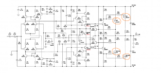
Now, am trying to build this amp. I think most of you are familiar with this amplifier or may not. Anyway. I've marked some driver transistor with RED color in the diagram. Question is, do these transistors require heatsink? Experts please clarify me on this area.
I've also marked the output mosfets with ORANGE color. Now the mosfets that have been used here are lateral ones. The place where I belong, it's very difficult to get lateral mosfets. So, one way ticket for me is to use vertical ones.
My second question is, if I really have to use vertical mosfets, are there any changes that I've to correct in this design?
Attachments
Yes the driver chain is current limited at 120mA or so at the cascode, suggesting heatsinks are needed.
You can't replace laterals without adding thermal bias stabilization circuitry. The
transconductance of VFETs is different too, so compensation is likely to be affected. The gate thresholds are different too IIRC.
You can't replace laterals without adding thermal bias stabilization circuitry. The
transconductance of VFETs is different too, so compensation is likely to be affected. The gate thresholds are different too IIRC.
Also the pinouts for laterals are different from VFETs, note, as the substrate is the source for a lateral, but the drain for a VFET.
Can I use power transistors instead of these mosfets here? Or what can be the possible solution if I want to keep the input and driver stage of this diagram?
If you want to build a similar spec. design with BJT output transistors, look at this fully supported design: The diyAB "Honey Badger" Class AB Power Amp - 150W/Channel – diyAudio Store
You can't replace laterals without adding thermal bias stabilization circuitry.
I think, but I may be wrong as well, the bias stabilization part already is present in the circuitry depicted at the beginning. Look at Q25 and mount this transistor to the driver and power device heatsink.
Best regards!
Careful. The doubled-up full-complementary push-pull LTP-VAS construction, with current mirrors at the load of the LTP, while looking good, lacks a determined and stable mechanism that decides the VAS standing current, other than the 120 mA limiter at the VAS collector circuit which is meant for protection instead. The VAS standing current is at the mercy of odds of randomness offered by the parameters of transistors being used.
This problem has been brought up many times in the forum. Many would ditch the current mirror for a simple resistive load. Bob Cordell has a good discussion in his book too where he offers a simple "patch-up" solution as well, by adding a shunt resistor across the current mirror to reduce the sensitivity of the VAS standing current to the "randomness". He traded for the VAS current stability with loss of the gain in the LTP stage.
I put that solution to test in my own Meistersinger amp project and it seems to have worked quite well. However in that project I used matched dual transistors for all the front end devices. I wouldn't know how well it would otherwise work in case if single transistors. The resistor value I used is 47K.
If you look at my posts #132, #186, and #190 in the Bryston 4B SST clone thread you will see that there are ways of stabilizing the vas current which do not involve any compromise of the input ltp/current mirrors and are pretty much independent of the vagaries of the components used. The vas current can be set easily and precisely. As you can see it works in real life as well as simulation.
If you look at my posts #132, #186, and #190 in the Bryston 4B SST clone thread you will see that there are ways of stabilizing the vas current which do not involve any compromise of the input ltp/current mirrors and are pretty much independent of the vagaries of the components used. The vas current can be set easily and precisely. As you can see it works in real life as well as simulation.
I'm afraid the only cure to that VAS standing current problem is a common mode feedback/control scheme that some of other member have proposed in the past and perhaps have tried/proven, which adds a considerably amount of complexity to the amp. Otherwise not much different from a "patch-up" solution like that of Cordell's, which dose effectively deal with the problem at little cost.
The hand-drawn schematic in #190 of Bryston-Clone thread probably would not work...the added pair of transistors common-based with the VAS transistors do nothing to equalized the VAS current between the NPN and PNP genders, as the common-based nodes are driven by the low impedance emitter followers ahead of them respectively, it makes no difference with or without the second pair of transistors after the VAS transistors.
You misunderstand the purpose of the extra transistors. The vas is one leg of a current mirror and the extra diode connected transistors are the other. The 2.7k resistor sets a 10mA standing current between the diode connected transistors and because the vas transistors are the other leg of the current mirrors then 10mA must flow between them too. I assure you that the prototype works as intended with very low distortion. This is exactly the same method of setting the vas current as used in the very successful Giovanni Stochino power amplifier - amongst several others.
By the way its not a "patch-up" ( not sure Bob Cordell looks at his design like that either ). The vas current can be set easily and precisely. If you looked at my post #186 you'd see pictures of the protoype and oscillograms of it in operation.
You misunderstand the purpose of the extra transistors. The vas is one leg of a current mirror and the extra diode connected transistors are the other. The 2.7k resistor sets a 10mA standing current ..........
Please take a hard look 🙂
https://www.diyaudio.com/forums/att...9837730-bryston-4b-sst-clone-mirrorvassch-jpg
.....It does that 10 mA only if the base were NOT driven. Seems to me you misunderstood your own circuit🙂
You misunderstand the purpose of the extra transistors. The vas is one leg of a current mirror and the extra diode connected transistors are the other. The 2.7k resistor sets a 10mA standing current between the diode connected transistors and because the vas transistors are the other leg of the current mirrors then 10mA must flow between them too. I assure you that the prototype works as intended with very low distortion. This is exactly the same method of setting the vas current as used in the very successful Giovanni Stochino power amplifier - amongst several others.
You're right, chalky, I spoke too soon. I put your circuit in LTspice and saw the action in working....I keep forgetting the high impedance nature of LTP current mirror load nodes.
Would you think the 2.7K reference setting current needs some heavy filtering? Is noise from the power rails a concern?
I suspect the posted schematic.
If anything because it uses the stabilizing "ballast resistors" on the *DRAINS* of output MosFets ... where they stabilize nothing of course.
That alone shows designer has no clue, and rather than designed from ground up, this is just a copypaste collage or a"mod" bases on other designs.
If anything because it uses the stabilizing "ballast resistors" on the *DRAINS* of output MosFets ... where they stabilize nothing of course.
That alone shows designer has no clue, and rather than designed from ground up, this is just a copypaste collage or a"mod" bases on other designs.
Yes nattawa you are correct the reference does need filtering, something like 47uf or 100uf across the 2.7k resistor should be sufficient. When I get around to implementing the real thing I'll probably use a two terminal constant current source rather than a resistor. You are also correct to voice concerns about noise from the power rails but the finished version will use separate stabilised supplies for each amplifier block, in the same way that Bryston do. There are a few refinements missing from the schematic I posted but I just wanted to try out a proof of concept design as quickly as possible. Thanks for taking the trouble to simulate the schematic.
- Home
- Amplifiers
- Solid State
- Amplifier Modification