Looks like two major updates to the schematic in one day! I took the discussion about short time constants benefiting power stages, and low ripple benefiting pre-amp and driver tube stages. Using the same part count as the previous version. I now have two variable PSU outputs, both track the variac. But the output on pin 2 is LCLC moderate ripple but a 6 ms time constant, intended for use by the power stage. And the output on pin 7 is LCLCLCLC, very low ripple but long time constant, intended for use by the driver stage. Please see schematic. Note on the amplifier side that the driver board is now being powered from pin 7 (low ripple) and the power stage is being powered by pin 2 (fast TC). This pattern of a Pi chain actually follows the traditional 1940's topology of tapping early off the Pi chain for the power tube and later off the Pi chain for the driver tube. Of course having two two differently characterized B+ sources available (pin 2 and pin 7) doesnt mean you have to use one or the other or both. If you were powering a pre-amp from this PSU you might only use pin 7. If you were powering a two stage amp like this you might use pin 2 for both the power and driver stages, or you might use pin 7's low ripple for the driver and pin two's fast TC for the power. I think having both characterizations of power available is good, and I had that extra spare wire in the umbilical, so why not!
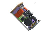
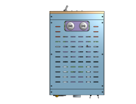
Iterations, iterations, I know. But now I think its done. I managed to decrease the depth by another inch, the box is now 13 deep x 8.5 wide x 6 high in inches, a manageable "power block" I can reuse with this amp and pre-amps, headphone amps, etc. Since it is variable. All point to point wiring occurs on the turret board in the middle, for easy servicing. The two boards near the front are the 6.3-0-6.3 dual regulated supply, and the gyrator choke parts for the bias supply, they are both heatsinked to the exterior via the thick slab sides. House ground and DC blocker board is on the back, the inrush soft starter is near the variac dial. The PSU side of the schematic is in-synch with these 3D models. I'm happy with it, I think it is assemble-able once I get all the chassis parts back. Below the tubes is another board that holds the diodes, the 5AR4 current limit resistors and the optional 0.1 uF input capacitor if needed. The 5AR4 sockets are actually 30mm above the sheet metal. Time to double check all the holes and start uploading metal parts for cutting and bending!
Attachments

Updated schematic. I realized the driver stage PSU output did not require the 300mA (Hammond 158T) chokes at only 1H, changed them to 150mA (Hammond 158Q) with more inductance 5H. Driver stage PSU output (pin 7) is designed for very low ripple and slow recovery time which pre-amp tubes like. Power stage output (pin 2) is designed for moderately low ripple but fast recovery time for the transients of a power stage.
I was wondering if you have introduced a lot of additional variables into the equation by also having the design aim that the PSU should have variable anode supply, and different current outputs, introducing some risk and a fair bit of expense.
Ultimately you will have a very nice 300B amplifier, so will you really want to reconfigure the PSU and commandeer it for other projects?
Ultimately you will have a very nice 300B amplifier, so will you really want to reconfigure the PSU and commandeer it for other projects?
will you really want to reconfigure the PSU and commandeer it for other projects?
If I live long enough, yes 😏 That is my intention, I'm not middle aged and I want to complete substantial projects before Jesus takes me home, not just the experiments and thrown together things I've managed so far. So it's about productivity too, a variable 300mA PSU with two outputs one smooth, one fast, as well as several low voltages, will cover the needs of many projects. With no effort other than turning the variac up or down. I am going to put a potentiometer shaft lock (Keystone makes them) on the variac so someone can't just go in there and crank the variac around maliciously. shaft locks are like a water line compression fitting, it grabs the shaft against the 3/8 nut. The current output of the pin 2 is 300mA enough for many power stages, pin 7 intentionally uses 150mA chokes so I can fit more henries and 150mA is plenty for many driver stages. Having the variac, to me, is the priceless aspect, as I don't have to buy transformers over and over and I can fine tune a project. So this is my thinking on all of this, in old age time becomes much more valuable than money, a variable PSU is about as productive in time savings one can get.
Moving on to updates to the amplifier chassis circuit since I'm pretty much happy with the PSU. Updated schematic.
Power section:
1) Added a grid balance control to aid in output tube calibration
2) Added a built-in panel meter and switch to aid in fine-bias calibration
3) Increased current sense resistors from 1R to 10R for better resolution with analog meters.
Driver section:
1) Depicted how you can use either an interstage transformer or a coupling capacitor to connect the driver tube to power tubes and still keep the direct bias circuit unchanged.
2) Indicated how to hook up a coupling capacitor or an interstage (designers choice) to the standardized terminals on the driver board. Turns out a coupling capacitor drops right in where an interstage used to be since the driver board has those terminals 1-4. For IT 1,2 = primary, 3,4 = secondary. For a capacitor short 1,2 and connect to left side of capacitor; short 3,4 and connect to right side of capacitor.
If you want to use capacitor coupling, must to plan -bridgeable- few hundred kOhm resistor between TP4 and coupling capacitor "output".
Capacitor coupled VAS stage requires appropriate anode resistor too.
Capacitor coupled VAS stage requires appropriate anode resistor too.
If you want to use capacitor coupling, must to plan -bridgeable- few hundred kOhm resistor between TP4 and coupling capacitor "output".
Capacitor coupled VAS stage requires appropriate anode resistor too.
Thanks again euro21, I felt I was forgetting something. I'll add those resistors to the diagram as the "capacitor option", next iteration. I truly appreciate your analysis.
The schematic was updated to correctly allow the driver board to use either an interstage or a capacitor to couple the output. This is accomplished by choosing one of two different jumper configurations on the driver board. One jumper configuration allows an interstage to be hooked to terminals 1-4. The other jumper configuration allows a coupling capacitor to be hooked to terminals 1 and 4.
euro21, if you get a chance would you look at this? I think I have it correct but would value your checking it.
euro21, if you get a chance would you look at this? I think I have it correct but would value your checking it.
- Home
- Amplifiers
- Tubes / Valves
- Ambitious direct bias PSE 300B with dual PSUs