Hi, I'm a computer engineer, I'm not a analog audio electronics expert but I'm some kind of DIY audiophile
I had this idea running in my head for a while, The things that I would like to have in the PCB was:
1. Space to use film capacitors and mica on audio path
2. Good filter capacitors on power secction
3. The best power supply
4. .1% Metal Film resistors
I know that many persons don't think capacitors and resitors make a difference in sound, but I do and for me is important.
So I ask for your help reviewing this design, I'm open to your suggestions in order to have a better design. I hope you can help me, this is my first PBC design 🙂
Attachments
- Read the datasheet very carefully, because the board layout is more important for performance than many of the parts. If you are not already using 4 layers, that's a good place to start.
- In most applications good quality modern C0G/NP0 MLCCs perform better than mica.
- In most applications 0.1% resistors are unnecessary. Go for low tempco instead of ultimate tolerance if you want to optimise.
- In most applications good quality modern C0G/NP0 MLCCs perform better than mica.
- In most applications 0.1% resistors are unnecessary. Go for low tempco instead of ultimate tolerance if you want to optimise.
Thanks for your recommendations, I read the Data sheet and I tried to make the same pcb design as they recommended and x7r ceramic capacitors in power filter.
but this is my first design and I don't really sure
but this is my first design and I don't really sure
Take a look at this thread: TPA3255 Reference Design Class D Amp GB there are recommendations on layout and inductors from several members with experience in working with the TPA.
Vmid cap use 470uF at least.
Vmid gnd, RCA gnd and power amp gnd should be star ground, preferable at the most noisiest ground point.
Vmid gnd, RCA gnd and power amp gnd should be star ground, preferable at the most noisiest ground point.

After you comment I studied the subject and I have made several changes to the design
I change my design to 4 layer
1 Signal
2 ground
3 Power
4 Signal
The power ground plane is separate from the signal ground plane as Texas Instrument recommends
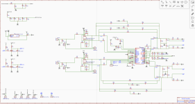
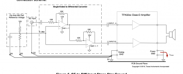
this is the design, What do you think?
I change my design to 4 layer
1 Signal
2 ground
3 Power
4 Signal
The power ground plane is separate from the signal ground plane as Texas Instrument recommends
this is the design, What do you think?
Attachments
Schematic seems good.
Please ensure the star ground do not connect the amp's pin directly. The amp ground should connect to a via to ground plane. The star ground should have another via to ground plane which was near the earlier mentioned via.
Nowadays layout are solid ground plane, splitting ground plane will have issues. Just ensure the digital are some distance away from the analog or high power and low power have distance between them.
If I route, I will do:
1. Signal, Power
2. Ground
3. Ground
4. Signal Power
This will ensure there's a ground return path below my signal or power.
JLCPCB cost USD 8 for 5 pcs 4 layer 100mm x 100mm board.
Hi Jasonhanjk
Thanks for the advice I will make the exercise.
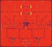
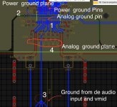
I tink I'm makin a mistake, because the star ground (number 3 in the image) is conected directly to the chip pin and then the chip pin is connected to the analog ground plane using a via(number 1 in the image)
All the capacitors and resistos are conected directly to de analog ground plane (number 4 in the image)
And then, the Analog ground plane es conected to de power ground plane using a via (number 2 in the image)
Thanks for the advice I will make the exercise.
I tink I'm makin a mistake, because the star ground (number 3 in the image) is conected directly to the chip pin and then the chip pin is connected to the analog ground plane using a via(number 1 in the image)
All the capacitors and resistos are conected directly to de analog ground plane (number 4 in the image)
And then, the Analog ground plane es conected to de power ground plane using a via (number 2 in the image)
Attachments
My routing method is power ground and analog ground is all flooded in layer 2 and 3, no separation. 😀
For star grounding, whether is my method better or yours. Normally have to use equipment to measure. Trial and errors many time then you would get it right. ;P
For star grounding, whether is my method better or yours. Normally have to use equipment to measure. Trial and errors many time then you would get it right. ;P
Hi,
I think that with the TPA3255 we must not neglect the importance of the inductors. In particular, I would focus my efforts on choosing the most appropriate one, to help you:

I think that with the TPA3255 we must not neglect the importance of the inductors. In particular, I would focus my efforts on choosing the most appropriate one, to help you:
Ground planes help to minimise stray inductance and RF pick-up / radiation by avoiding large gaps with voltages across them. So I'm not sure how well a star ground would react if if it's next to a digital ground plane.
Maybe 'star' it in the sense that you pick a good reference point/s, both between components and on the board to minimise current and connect multiple planes with 0ohm resistors.
I concur with using good quality caps. X5R or better with a generous voltage rating to minimise voltage-dependent capacitance modulation. And avoid polymer caps except for non-audio PSU parts where high leakage is not a concern.
And if you want to go all-out, consider metal/alloy powder inductors instead of ferrite. It may be a non-issue because the switching frq is RF, but it's still being demodulated to audio frequencies, so hysteresis related memory will probably create noise.
Thanks all for your comments,
I made a change on the order of the layers after reading your comments and reading online articles about the different options available
1 Groud
2 Signal/power
3 Signal/Power
4 Ground
I bought all the parts from mouser.com, unfortunately I did it before reading the last comment about powder inductors instead ferrite, I purchase this one, SER2915H-103KL Coilcraft | Mouser
240 Dollars only in parts!!, I don't know how Chinese companies achieve these prices on complete boards
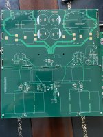
Attachments
Last edited:
I‘ve demonstrated that 2 layers is possible.
So if you go 4 layers, are you sure about your build-up?
IMHO, signals, power planes, power planes, signals, is the way to go?!
JP
So if you go 4 layers, are you sure about your build-up?
IMHO, signals, power planes, power planes, signals, is the way to go?!
JP
Hi JPS64
what I have learned in this project is that pcb design is a serious business and I admire all of you that are in charge of this job.
I'm a software engineer and in my field is the same thing, you can apply different techniques to resolve a problem, the techniques depend of your experience, tools, and technical skills.
Too be honest I'm not 100% sure about the planes distribution, but, as far all the technical documents that I have read, I think is the best way.
4 Layer PCB - Stackup & Prototype | ALLPCB
Common PCB Stackups for a Four-Layer Board - Technical Articles
I'm a hobbyist, this is a personal challenge to create some thing completely at my taste using all the advantages of this time (free tools, pcb fabrication, etc)
But I'm aware that this is serious field that's why I´m looking for advice before order the final PCB
Thanks all for your time
The most expensive part in the bom should the amp IC and inductor, the rest of the parts you had choose are way overpriced. 😀
Having signal in layer 2 and 3, there would be crosstalk between signals.
Having signal in layer 2 and 3, there would be crosstalk between signals.
Hi Jasonhanjk
Thanks for your comments, after thinking I change my mind and I will use
1. Signal
2. Ground
3. Ground
4. Signal
I think is the safest distribution to use
I know that the components that I bought are expensive, but this is the point of this experiment, I have a idea fixed in my head about the real difference using this kind of components and hear the real experience by my self and build my own opinion.
🙂
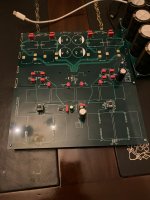
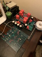
Hi all
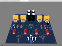
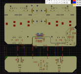
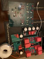
just to thank all of you that help me with your comments, this weekend the board arrived and start to make some progress
I change the original project and added two active crossover, those already tested and worked fine, now the amp is taking shape
just to thank all of you that help me with your comments, this weekend the board arrived and start to make some progress
I change the original project and added two active crossover, those already tested and worked fine, now the amp is taking shape
Attachments
- Home
- Amplifiers
- Class D
- (Almost) cost no object class d TPA3255 design, help