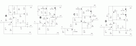
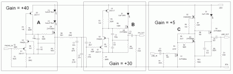
Here are the gain cells used (or contemplated) for this go-round. Cells A and B are used in the RIAA section, A for the input, and B for the output. C is a buffered "Fake SIT" feedback pair that I've used as a line stage (5X) in another version of this preamp - it acquits itself well. For those who think that interstage coupling caps are the Devil incarnate, cell D is a direct coupled version of cell A that gets rid of the interstage cap. Cell D has been simulated (it simulates nicely), but hasn't been built yet. All of these cells use feedback.
Questions? Ask.
Questions? Ask.
Attachments
Here's the latest All-In-One Preamp lash-up that will likely make its way to BA 2015. The phono section is appropriate in gain for a MM or high output MC cartridge, and the phono input is terminated with a reasonable starting resistance (so I'm told) to handle a Denon DL-160 high output MC cartridge, a beast I'll be trying soon.
All the gain cells in this go-round incorporate feedback, so channel - to channel gain matching is very good. Also, the RIAA response should be well-matched between channels.
In the schematic I show the basic gain cells, along with equalization/compensation, but not the bypassing and accompanying on=board shunt regulator.
Later, I'll show the gain-phase plots for each section.
Attachments
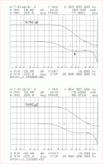
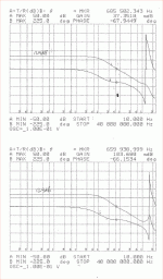
Here are the gain-phase plots for the 40X phono front end. I'm still trying to figure out why is gain crossover is so different between the two channels. This won't keep me, however, from throwing it into a box and giving it a listen.
Attachments
Last edited:
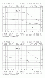
Here's the gain-phase for the 30X phono output stage. In this case, the gain crossover frequency is similar for both channels. In both cases passband gain matching is excellent. The penciled-in values for gain were taken at 1 kHz in all cases. The droop at low frequencies is a 10Hz pole introduced for rumble filtering.
Attachments
I just did some substitutions on the front end RIAA stage of the latest All-In-One that may straighten out the differences in gain crossover frequency as well as make the stage easier to build in the long run. I'll find out if my surmise is correct tomorrow or Monday.
The preamp finally got a listen last Wednesday and was on the job all day long at Burning Amp 2015 handling a Denon DL160 high output MC cartridge and switched between 4 completely different power amplifiers. I was pleased with the results in each case, and so were a bunch of other folks who dropped in over the course of the day to listen.
Hi,
congrats to that nice circuit.
You know I like Your designs and the CFPs in special ... so I decided to sim the circuit.
So far sims look well, but three points made me wonder:
- The idle currents of both Phono-gain-stages run on low values.
4.4mA for A (900µA the JFETs, 3.5mA the MOS) and 4.2mA for B (600µA/3.5mA).
Do the praxis results differ, or are those low values chosen for a purpose?
- The results for the Line-level stage are clearly different.
Here the Transistors idle on much higher levels: Q1: 8.6mA, Q2: 14.2mA, Q3: 5.6mA and Q4: 34.7mA.
- and lastly: When Joachim Gerhard built my Calvin-Buffer with MOSFET output transistors (similar to gainstage A and B) he experienced large offsets, hence the MOSFETs would have required very precise matching.
Since You don´t degenerate the output MOSFET sources, had You any issues regarding the bias points?
Or does feedback control (or hide) possible issues here?
jauu
Calvin
ps. if You like I could attach the LTSpice sim-file.
Hi,
just btw: funny -or rather a bit astonishing- is at first glance, that the current through the input MOSFET M1 of the LineLevel-stage is out-of-phase with the input voltage, even though it acts as a source-follower, hence it´s drain voltage, resp. node-voltage @R3/R4/R5 is in phase with the input.
Of course seen current-wise from the CCS M3 it becomes obvious that the difference current between CCS and M2 flows through M1 (and M2 together with M4 beeing the dominant parts here).
But that brought me to an idea.
It should have a positive THD-reducing effect, if the voltage-drop over R3, M1´s Source-resistor could be held constant.
There are two ways to do so.
a) connecting a E-lytic of ~100µF in parallel to R3. Beeing always positive polarized a E-lytic suffices fully here.
or b) replacing R3 by a LED of similar voltage drop ... green would be ok here.
Indeed resulted the simulation in a drop of the THD-value by ~6dB.
The LED giving better results, especially regarding the H3-value (~10-12dB difference)
jauu
Calvin
Last edited:
- Status
- Not open for further replies.
- Home
- Source & Line
- Analog Line Level
- All-In-One Preamp Circuit