It's been a while, but I finally got around to making the changes to tame the line amp. I ended up with a somewhat simpler circuit than the one proposed in post #11, and it wasn't all that hard to compensate, requiring that I merely change a resistor value at the input. I'll post the schematic when I get around to modifying it, but here are the gain-phase plots - plenty of gain and phase margin. Look for the schematic soon. I now have some incentive to finish wiring up the test box and give this thing some living room time.
Attachments

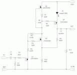
Here's the line amp circuit I'm going with for the time being. Its G-P plot is shown in the previous post. Resistor R2 works against the input capacitance of Q1 to provide the pole that compensates the circuit.Though the overall gain-phase looks good, I think it might be better to plant the compensation pole farther inside the loop, say at R4 or R8 instead of R2. I'll hold that thought for a bit though, as I'm tired of messing with this thing and want to listen to it for a while.
Attachments
This setup finally got installed in the living room last night. Line amp sounds nice - the phono amp as well, but there is some "rush" noise coming from the phono preamp. This may be a noisy gain stage or power supply (I used an augmented TL431 shunt regulator that may not have the best noise performance). There might also be an oscillation issue requiring some creative compensation.
In many ways. I'm very happy with the preset setup, except with the slight "rush" noise in phono, only audible when close to the speakers. I was using a Creek phono preamp clone previously, and was never very happy with the lack of bass and the inverting nature of the Creek circuit that makes the phono opposite in phase from any other source. I've pretty much made up my mind that I won't bother any more with any phono preamp that's not non-inverting.
At my leisure, I'll dig out the source of the noise, though it's never audible where I listen.
At my leisure, I'll dig out the source of the noise, though it's never audible where I listen.
As far as the rushing noise is concerned, I think it might be inner loop oscillation in the shunt regulator. TL431s are notorious for squirreley behavior, like peak detecting RF noise and taking off in oscillation at a few MHz on a whim. The parts are variable from one manufacturer to the next, as each vendor has a somewhat different take on the design necessary to meet the black-box specs of the part as originally conceived by Texas Instruments back in the 80's. I've suffered with the quirks of the TL431 for well-nigh on to 30 years, as it is the de facto standard for reference/error amp duty in SMPS circuits (my bread and butter). At any rate, the major loop for the shunt regulator was stable in simulation. This does not mean that an inner loop is not misbehaving in some manner. The model for the TL431 in PSpice may not mimic the behavior of the TL431 I'm actually using (NSC before the TI merger). I suspect I might need a compensation cap around the TL431, even though the simulation did not show a requirement for such, especially as I have tarted up the TL431 with a current source load, giving it a lot of gain and practically begging it to misbehave.
Edit - What does this actually mean in practical terms? I'll be looking at removing the lead cap (C10 in the schematic at the beginning of this thread) and replacing it with a small lag cap from cathode to reference of the TL431. This shunt regulator would probably benefit from a session with the HP4194A gain-phase analyzer at my workplace, assuming I can figure out a good place to break the loop for measurement.
Edit - What does this actually mean in practical terms? I'll be looking at removing the lead cap (C10 in the schematic at the beginning of this thread) and replacing it with a small lag cap from cathode to reference of the TL431. This shunt regulator would probably benefit from a session with the HP4194A gain-phase analyzer at my workplace, assuming I can figure out a good place to break the loop for measurement.
Last edited:
Wrenchone,
I would be I interested to know what the permanent fixtures are in your system. Your reference point.
I would be I interested to know what the permanent fixtures are in your system. Your reference point.
At present, my system consists of a Kenwood 2055 TT with Grado Gold cartridge, A Calfornia Audio Labs CL-15 CD player, Event 20/20 monitor speakers, and my "Le Mutant" Class A power amp, now that it has been retooled so that it doesn't overheat. I might be upgrading the TT soon, and will eventually transition to a Denon DL-160 high output moving coil cartridge. The amps get swapped out regularly, but I think the Mutant will be in my current lineup for a while, as I am very pleased with its living room performance. It also has distinguished itself at the 2011 and 2013 Burning amps. Speaker and interconnect cables are nothing special.
Last edited:
Forward - Into the Past!!!
The next stab at an all-in-one preamp solution starts with a folded cascode circuit that was more or less shoved in my face quite a few years ago in the course of the "Open Loop Follies Thread". This circuit will serve as the input half of a passively equalized 2 stage RIAA preamp. Some bows and ribbons were added to improve supply rejection and increase the output impedance. Gain is around 40x, and simulated distortion figures are not bad at all. This and the succeeding circuits (wait for them, they will come) have been laid out and are waiting for me to free up some time to actually build them. The voltage source feeding the cascode transistors/fets in this circuit will be a string of GaAsP deep red LEDs.
Next up will be the second stage of the RIAA preamp.
Attachments

Last edited:
Here is the RIAA second stage, utilizing a common source amplifer with cascode, augmented with a current source to increase the bias current of the gain device, lowering THD. I started out with a 2N4391 jfet as gain element, but switched to a BSS159 depletion mode mosfet (available from NXP) which has lower THD with less bias current.
Gain is ~30X, and the distortion simulation was performed with enough input signal to drive the output close to 1V. Lower drive levels result in less distortion. I may or may not add a source follower buffer, as the output will drive only a 50k pot. Any interface to the outside world will be via a hefty line amp, detailed later.
Gain is ~30X, and the distortion simulation was performed with enough input signal to drive the output close to 1V. Lower drive levels result in less distortion. I may or may not add a source follower buffer, as the output will drive only a 50k pot. Any interface to the outside world will be via a hefty line amp, detailed later.
Attachments

The next stab at an all-in-one preamp solution starts with a folded cascode circuit that was more or less shoved in my face quite a few years ago in the course of the "Open Loop Follies Thread". This circuit will serve as the input half of a passively equalized 2 stage RIAA preamp. Some bows and ribbons were added to improve supply rejection and increase the output impedance. Gain is around 40x, and simulated distortion figures are not bad at all. This and the succeeding circuits (wait for them, they will come) have been laid out and are waiting for me to free up some time to actually build them. The voltage source feeding the cascode transistors/fets in this circuit will be a string of GaAsP deep red LEDs.
Next up will be the second stage of the RIAA preamp.
So, let me see if I follow. You have a common drain gain stage, loaded with a jfet CS, feeding a folded cascode, that is cascaded as well. What is the other jfet at the output? Ah, it is the CS for the voltage reference the cascaded devices are using.
A folded cascode circuit essentially acts a a current divider, partitioning a fixed current between the gain device and the output load resistor. In the simplest implementation of the folded cascode, a resistor is used as the current source that is partitioned. If that resistor is clamped with a voltage source at the cascode transistor, it can work pretty well from the standpoint of linearity, except for ripple rejection.I chose to use a p-channel jfet as a current source instead of a resistor to increase ripple rejection. It's not a load for the gain transistor.
The folded cascode circuit partitions current between the gain device and the output load resistor. I wanted the cascode transistor feeding the output load resistor to have as high an output impedance as possible to avoid RIAA equalization errors, hence the inclusion of a very "pentody" small-signal mosfet between the initial cascode transistor and the load resistor. The RIAA equalization network will go across the load resistor - the closer to a current source (read high output impedance) feeding this resistor, the lower the RIAA equalization error that must be trimmed out in subsequent testing.
I have another revision of this circuit that will be posted soon. The voltage across the PN4393 gain fet has been reduced to lower its power dissipation to levels that could be reasonably expected for a TO-92 device sans heat sink. The THD and distortion spectrum (at least in simulation) is essentially unaffected.
The link to "open loop follies" in a previous post does not work now. This one should work a lot better...
http://www.diyaudio.com/forums/analogue-source/49673-open-loop-follies-pt-1-a.html
http://www.diyaudio.com/forums/analogue-source/49673-open-loop-follies-pt-1-a.html
Last edited:
This is a revised version of the folded cascode circuit the reduces the power dissipation in the input jfet to a value resonable for a TO-92 device without heat sink. The current delivered by the J175 current source was reduced, and the voltage at the base of the cascode transistor was reduced to cut the power dissipation on the input jfet while keeping its bias current the same.
Attachments

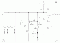
Here's the last bit - a line amp with gain. In this case, it's about 6X. I find it hard to believe the simulated distortion, but I betcha in practice the measured distortion will still be pretty low. I may try a teensy bit of DC bias at the input to swing the quiescent output voltage closer to VCC/2. Then again, I may not. Food for thought...
Attachments
I've been putting up with the noise from the phono stage for a while - puts me in mind of a muted version of a leaky toilet - all hiss and very little hum. I'm beginning to think it was a big mistake to base the shunt regulator circuit on a TL431, as they are pretty noisy. I have a new design for an "amplified zener" shunt regulator using a pair of GaAsP red LEDs as a reference that looks very good in simulation. This will be built up on a piece of perf board and bodged into the current test board to replace the old shunt. I suspect this will go a long way toward quieting things down, as I have other boards with quieter shunt regulators that don't hiss like this one. I'm probably going to take what I've learned in this exercise and start another thread on fast, low impedance, low noise shunt regulators.
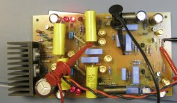
I bodged a new, quiet shunt regulator using an LED reference into the power supply section of this board, replacing a TL431-based circuit that looked elegant in terms of convenience and parts count, but ended up as a hiss factory. TL431s are noisy - they'll go back in my parts box and only get used where their high noise doesn't matter. I'll show the new regulator circuit here, but it'll get discussed in detail in another thread re low-noise regulators I have running in "Analog Sources", especially now as the new circuit has earned its chops as low noise - hiss, begone...
Here's the new regulator that's in there - nice and quiet. It'll get described in more detail in due course in a thread on low noise regulators I have running in the "Analog Sources" section of this site.
For contrast, the previous regulator shows up in the first post to this thread. I won't even bother to describe it in detail, as it is fatally flawed noise-wise. I'll just consider it a "what the He**was I thinking!" episode, and move on.
For contrast, the previous regulator shows up in the first post to this thread. I won't even bother to describe it in detail, as it is fatally flawed noise-wise. I'll just consider it a "what the He**was I thinking!" episode, and move on.
Attachments
Last edited:
- Status
- Not open for further replies.
- Home
- Source & Line
- Analog Line Level
- All-In-One Preamp Circuit