Don't feel bad about getting confused by different systems, even rocket scientists do it some times.
NASAs metric confusion caused Mars orbiter loss - CNN
😛 We are human, not martian.
That is good hint. I think I could replace those coupling caps easy without desolder any bridging wires. Yea, my major concern was bass and now plus the hot pad issue.not that there's anything wrong with replacing all the caps in your amp, but if you want to save a few bucks you might try replacing the small caps first and see if that solves your problem. the smaller DC blocking caps in the signal path will cause a loss of low end when they start going bad, which sounds like the problem you started describing. when the big filter caps in the power supply go bad it will cause hum and buzz problems in your audio due to ripple appearing on the power supply rails.
-Joel
ZM also suggest using 470uF instead of original 220uF. I would like to learn the pros & cons of those choices.
Thanks!
ZM also suggest using 470uF instead of original 220uF. I would like to learn the pros & cons of those choices.
higher capacitance here means a lower corner frequency. not much downside to using higher value, except for the physical size of the package. Also, even though there is probably a low DC across these caps, a cap with a higher voltage rating will tend to have a lower ESR, which can be advantageous. get like a 470uF 50 volt cap, if you can fit it on the board.
-Joel
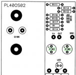
Now I have some issues for coupling caps. The space for them is really tight. If I put them upright only 10x15mm (DxH) caps can in on the boards for C102 & 103.
If I get Elna RFS, they are easily 10x20 ~ 16x30mm even just 220uF. Hugh!
The current idea is to
* solder the cap (C101, 102, & 103) horizontally with bent leads
* solder on cap (C103) on the correct side of PCB and the other (C102) on the wrong side of PCB
Such horizontal way also move C103 away from bare alumina heatsink.
Or I can use Nichicon 220uF/50V, 105F and they are 10x10mm without any of those problem. 440uF caps are just too big and have to use the horizontal scheme.
High capacitance also has higher ripple current, does that matter for these coupling caps?
What is your suggestions? Thanks!
Attachments
Last edited:
you have 3pcs of 220uF caps per channel , according to schmtc
C101 and C103 are more important than C102
so - for C101 and C103: in your boots I'll solder some fine MKC (polycarbonat) of 10-100nF on "right side" , and fine Elna Silmics on copper ( inner ) side of pcb
for C103 - either use Silmic again or any other decent cap , but you can solder it on any side , depending of dimensions
not really big fuss
ZM, some more hint, please. What's the purpose or scheme of using those MKC caps? to provide leads to the "back" (copper) side for Silmics cap? I am lost here.you have 3pcs of 220uF caps per channel , according to schmtc
C101 and C103 are more important than C102
so - for C101 and C103: in your boots I'll solder some fine MKC (polycarbonat) of 10-100nF on "right side" , and fine Elna Silmics on copper ( inner ) side of pcb
Actually C101 was the one by itself. I can use large one if lay it horizontally. (or with your scheme if I can figure out what you meant)for C103 - either use Silmic again or any other decent cap , but you can solder it on any side , depending of dimensions
mkc are for bypass - sort of speed-up buddies for electrolytic caps
through C101 and C103 you have signal flow ; C102 have sort of other role
through C101 and C103 you have signal flow ; C102 have sort of other role
Got it. Last time I got advice on bypassing the power filtering cap and found the treble became more stressed than what I like. Then I read some debates on this topic. I guess it makes more sense to try it on coupling caps (C101 & 103, right?)
I finally settle down to Elna caps with biggest size allowed in Aleph3. They all will need to be mounted on the back side of PCB. Also got some Panasonic power filtering caps. But again due to the diameter and lead spacing limit, I can use up to 33mF/25V.
This brings another question: can I find some DIY PSU board that allows larger caps and still can be fit in Aleph 3? And does DIY Pass Lab amps take liberty to have PCB that allow generous sized components?
Last edited:
.......
This brings another question: can I find some DIY PSU board that allows larger caps and still can be fit in Aleph 3? And does DIY Pass Lab amps take liberty to have PCB that allow generous sized components?
leave it as is - with original pcb
if you want better - you need to go with complete dual mono route , with Jfet front end - say as Aleph J or Babelfish J ( my shameless knock-off of original)
recapping it , with increased PSU caps is max you can do in that case ;
changing it too much would be blasphemy , without substantial benefits
so - conclusion - finish what you already intend to do with original one , and - if you want better - build two mono blocks , from scratch
Yes, that is probably good idea. I don't want to end up with a Frankenstein 3. 😀
I have been thinking building one (Aleph J or 5) with 50~60W/ch long ago. Just need to find out where to buy the heatsink and PCB...
I have been thinking building one (Aleph J or 5) with 50~60W/ch long ago. Just need to find out where to buy the heatsink and PCB...
Desolder thick wire
I need some help to desolder the thick wire.
I am using my 45W Aoyue 937+ solder station and 2mm flat tip. I tried tip temperature from 300~400C. Some thick wire just come out easily, but some just stick to the pad. The solder was like thick jelo and wouldn't flow well. I don't have flux so just use a little fresh solder to help heat conduction. I got some old solder melted and sucked out, but there was some hard "solder?" at the tip of the wire just can not be melted or removed. I have spent more than 30 min on that specific wire. And really appreciate some help! That was the wire connecting the PSU board and negative speaker post.
Thanks!
you need more soldering power , both electrically and mechanically
45W is almost enough , but not with 2mm tip
45W is almost enough , but not with 2mm tip
OK, I'll took it to my research lab for some real power. 🙂
The wire I had problem actually was a ground wire. The pad on PSU board has huge surface area and hence big heat sink there. That is probably why my iron didn't work.
The wire I had problem actually was a ground wire. The pad on PSU board has huge surface area and hence big heat sink there. That is probably why my iron didn't work.
Still not working...
I tried the Metcal MX-500 (40W? biggest one I can find) with bit tip at work. Lots of flux, plenty of new solder to flood the joint (in case lead free solder was used), still I cannot desolder the power cap leads, which also has plenty copper on PCB.
I can clean most the solder out, but the PCB was quite thick and there are still some residual solder stay at the base of the leads. I tried to wiggle the cap, no moving at all. I never had so much trouble with desoldering. I guess the ground plane was the problem.
I found some 60W watt solder station with plenty tips, or this 70W one with bigger tip. Or should I just buy some >100W gun? Or should I pre-heat the whole PCB board with hot air gun?
This is really frustrating! Thanks a lot for help!
simple
just example - I'm using for chunky work plain 220V Iron - 60W , base of soldering tip around 8mm dia , 12mm wide screwdriver type
never needed to use bigger one , while working on pcbs
just example - I'm using for chunky work plain 220V Iron - 60W , base of soldering tip around 8mm dia , 12mm wide screwdriver type
never needed to use bigger one , while working on pcbs
simple
just example - I'm using for chunky work plain 220V Iron - 60W , base of soldering tip around 8mm dia , 12mm wide screwdriver type
never needed to use bigger one , while working on pcbs
My current problem was not able to get the cap out. The power cap was just stuck there. When I replaced the coupling caps, they are very easy to desolder: small pads, little solder. As soon as I suck out most of solder, the cap can be wiggled out by heating one pad at a time.
But these big power cap and thick wire just don't move even there wasn't much solder there and the residual solder was flowing! I even suspect that there is some solder "in the through hole" and since the hole is deep (thick PCB) there might be solder there didn't get any heat and still solid???
Again, I have no problem to remove most solder now. However, the caps or thick wire were just stuck.
simple
just example - I'm using for chunky work plain 220V Iron - 60W , base of soldering tip around 8mm dia , 12mm wide screwdriver type
Just noticed that the tip (12mm) you mentioned is even wider the base diameter (8mm)?
Why use such wide tip? Although the pad is about 5 mm, the lead at the center was always in the way so I can not even use the whole width of the tip (or I'll burn the PCB).
Or you use that extra wide surface area to draw the solder out of the pad?
Now I am pondering if I should get the 70W soldering iron or >100W soldering gun to do the job. In my discussion with my staff, it seemed that the wall of the through hole on the PCB has conductor so the solder may actually bound the lead along the through hold, so I definitely need fast dump of thermal power to melt solder there.
dimensions - I wrote them to give you illustration about thermal capacity of iron ;
for heavy soldering you need massive tip , besides substantial electrical power
anything less than substantial sized tip will loose temperature rapidly , and all you will be doing is just heating pcb , risking damage and de-laminating of traces from pcb base
for heavy soldering you need massive tip , besides substantial electrical power
anything less than substantial sized tip will loose temperature rapidly , and all you will be doing is just heating pcb , risking damage and de-laminating of traces from pcb base
Thanks for the hint. I'll try the larger thermal mass route. I will try some blocky tip and even some butane soldering iron today. 🙂
to ease removing wire from pad ( then cleaning pad from solder is piece of cake with solder sucker ) - add some new solder to connection , to achieve better and faster transfer of heat from iron
- Status
- Not open for further replies.
- Home
- Amplifiers
- Pass Labs
- Aleph3 recap