OK, still confused. I've ordered the DC-DC Boost, but in the interim, I used a bench supply at 52Vdc input to the motherboard and adjusted to get 48V at the drain on the MOSFET on the daughterboard. I can still only get about 18Vp-p, with a 1Vrms 1kHz sinewave applied to the input. Above that it clips one side of the output noticeably (negative peak on my 'scope).This preamp was designed to work with 48v Vcc so about 52v upstream of the cap multiplier and CRC supply to account for drop out. What I use is a DCDC step up supply powered by a 12v 1A linear Class 2 wall wart. The 12v is boosted to 52v or so with the trim pot. Measure the voltage at the drain of the mosfet and adjust trimpot until it reads about 48v. The circuit DC setpoints was not optimized for 24v or 36v. It can work there but you won’t get anywhere close to 40Vpp output.
Will appreciate any suggestions
It sounds like your DC setpoints are off and your output node is far from midpoint of approx Vccc/2 (~24v). If asymmetric it wo t clip evenly. This might be because you used a different MOSFET? Or more, likely, one of the resistors is the incorrect value. Please provide some clear closeup photos of the daughter board so we can see the parts and construction.
Please measure the delta V (and hence bias current across the input pair and also the output stage. Convert that to mA.
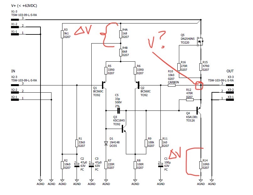
Please measure the delta V (and hence bias current across the input pair and also the output stage. Convert that to mA.
Problem Solved. As it almost always is, (at least in my case) it was a stupid mistake.
As you suspected, it was incorrect resistors. Not incorrect values but incorrect installation. R3 and R4A were crossed. Despite your warning about following the "tails" on the resistor markings, I had those two incorrectly installed - on both daughter boards.
Now I'm able to get 44Vp-p with 8.4Vp-p input and 24Vp-p with 3Vp-p input (the outputs of my signal generator, so everything seems to be well.
Now to get the PSU revised and into a case so it can power my F4.
Many thanks.
Great news!
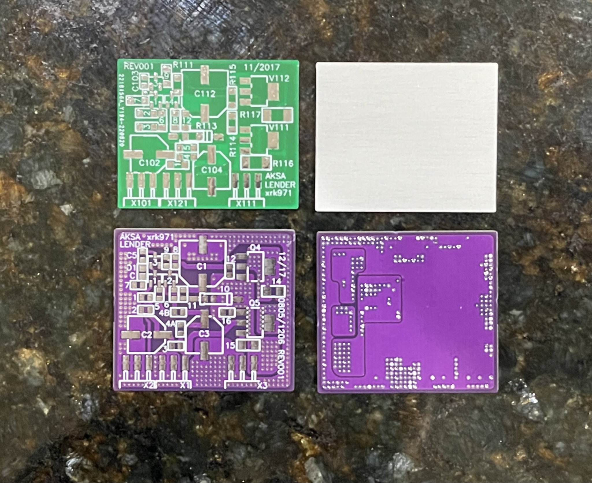
I just got a batch of cool looking purple 0805/1206 SMT and some green aluminum IMS SMT daughter boards. There are in my shop and ready to ship.
The IMS allows you to stick it to a heatsink (chassis floor or side wall) and run extra high bias current for driving headphones etc. Maybe even a heavy load like a 2W headphone. You can sink a lot of heat with these.
Last edited:
I have recently completed construction of the AL preamp (TH DB's) using standard BOM component values. Listening for several hours has confirmed for me the favorable comments that have been posted - its an absolute cracker. However, my build has a fault, the solution for which has proven to be elusive for me. On initial power up and for about 20 minutes of operation, it is dead quiet. After it has fully warmed up, noise and hash (possibly resembling the sound of RFI?) becomes audible and remains constant but not getting louder beyond annoying background level. I am running a Meanwell LRS-150-36 SMPS into the DC-DC converter suggested by X, then CLC filter and switch. I'm reasonably certain none of these as well as the cap Mx are the cause of the problem. Input voltage to CLC filter is 52.3V and there's 48V after cap Mx. Ripple after R147 is < 0.5mV (measured with Fluke 87 DMM). I have tried a range of grounding configurations, none of which yielded improvement. I'm confident it isn't a grounding issue.
My thoughts at present are that the noise is thermal as it is only present when the preamp warms up. Vcc/2 is ~ 25V. I have not measured delta V across R4A and R14 but Q4 and Q5 are running warm (not hot) so I presume current draw is isn't excessive. Is it possible these (or other Q's?) could be producing excessive thermal noise? Interestingly, the noise level is similar in both channels.
Any thoughts or suggestions regarding what the problem may be, or any further investigations I could undertake to solve it, would be greatly appreciated.
Thanks in advance.
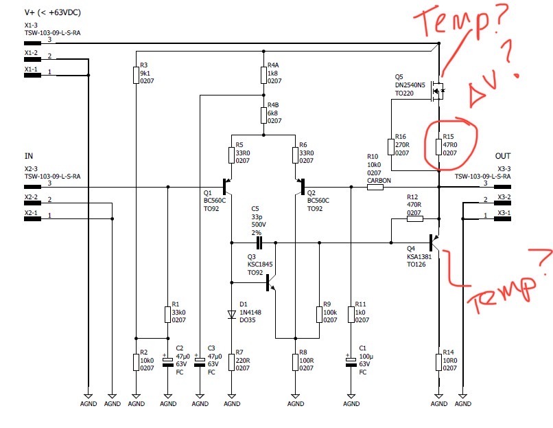
This is a strange one. I have not had any problem like this. If it is thermal, it might be caused by insufficient heatsinking of the outputs. Or an incorrect resistor value leading to an excessively high bias current that makes the outputs too hot and they degrade. Can you show a photo and tell me how hot the DN2540 and KSA1381 heatsinks get? I am assuming you have the through hole variant. Also, please measure the voltage across the source resistor (R15)of the DN2540 so we can calculate the current.
Also, if you have a linear 12v 1000mA wall wart (like those used on old WiFi routers), try that as the supply to the DCDC step up PSU.
Also, if you have a linear 12v 1000mA wall wart (like those used on old WiFi routers), try that as the supply to the DCDC step up PSU.
Thanks for your suggestions. I will try them and report results.
Neglected to mention - Q5 is DN2535N5 as DN2540N5 was not available. Only significant difference I can see is former is 350V & latter is 400V. Also, I have tried 24V DC (from Sigma 11) to both step up PSU and direct to CLC input with same results ie. noise persists.
Thanks again.
Neglected to mention - Q5 is DN2535N5 as DN2540N5 was not available. Only significant difference I can see is former is 350V & latter is 400V. Also, I have tried 24V DC (from Sigma 11) to both step up PSU and direct to CLC input with same results ie. noise persists.
Thanks again.
That sounds like a thermal issue then or perhaps a cold solder joint that heats up when running full current.
Rolotube,
Can you post clear detailed pics of the main board and daughter boards?
How are the DB's mounted to the main board, socketed or soldered direct?
Can you post clear detailed pics of the main board and daughter boards?
How are the DB's mounted to the main board, socketed or soldered direct?
After about 40 minutes of operation:
Temps - Q4 ~ 48 degrees, Q5 ~ 35 degrees. L and R channels within a degree or two of each other. Neither Q4 nor Q5 has a heatsink.
Delta V's - R4A (1K8) = 4.68V, R14 (10R) = 0.232V, R15 (47R5) = 1.152V, R147 (0R33) = 0.0202V. L and R channels within a few mV's of each other. So by my calculations, input pair bias current is 2.6mA, output stage is 23.3mA and Q4 current is 24.3mA.
I have re-checked component values and placements, all looks OK.
Cold solder joint is a possibility but would have to be on main board as noise is common to and fairly even in both channels. I'll reflow entire main board to eliminate this. Thanks again for this suggestion. DB's are socketed.
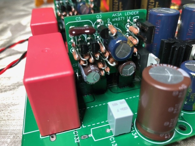
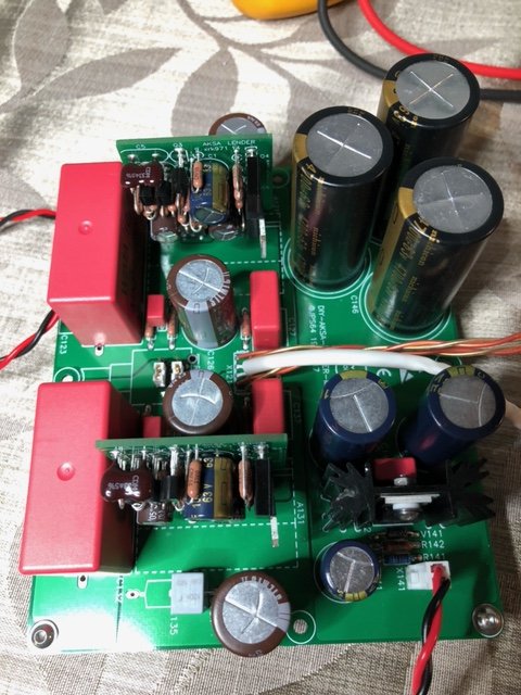
The dissipation all looks good and about 0.5W on the outputs so should be fine - but adding a small stamped aluminum fin heatsink wouldn’t hurt.
Are all of your electrolytic caps mounted with correct polarity and DC voltage rating?
Are all of your electrolytic caps mounted with correct polarity and DC voltage rating?
I've checked polarity and voltage of electro caps, these are OK. Reflowed solder joints on main board and replaced bypass caps C125 and 135 (Vishay MKP1837, I thought they may not have been up to the job). No improvement. I then removed R147 and connect V+ (48V DC) directly to C1048. This bypasses CLC and cap Mx, just in case problem was with these. Same result, noise persisted as before. So it appears there may be an issue in both DB's. Possibly wrong component placement or value? As best I can, I have visually checked these and they appear OK. Also, you've indicated that critical voltages and currents are pretty much OK. Short of systematically replacing DB components (which would be a time consuming and tricky process), I don't know where to go from here - this has me stumped!
After reading about excellent results with SMT DB's some time ago, I ordered a set (as well as a spare set of TH) which should arrive soon. I'll build these up and see if the problem persists. If not, the problem is with existing DB's. If it does, I may need to rebuild the main board from scratch (or replace). I hope this can be sorted one way or another as the brief noise-free listening I've had to date confirms that the preamp is very much worth persisting with.
Many thanks again for your assistance.
Hi Rolo,
Sorry you are having so much trouble. It sounds like a thermal problem and all I can suggest is to add a small screw on stamped aluminum heatsink to the mosfet and BJT.
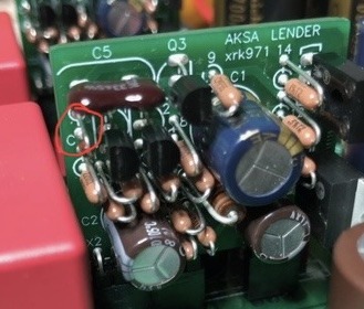
Can you confirm that the cathode on your diode faces the correct direction (towards the “C”)?
Another way to test if thermal effect is to set a fan blowing across the DBs. If the problem does not come up after 20min, heat is the culprit.
Sorry you are having so much trouble. It sounds like a thermal problem and all I can suggest is to add a small screw on stamped aluminum heatsink to the mosfet and BJT.
Can you confirm that the cathode on your diode faces the correct direction (towards the “C”)?
Another way to test if thermal effect is to set a fan blowing across the DBs. If the problem does not come up after 20min, heat is the culprit.
twocents - Q4 is KSA1381. I will try a heatsink. Q4 is currently mounted on top side of PCB where there isn't clearance. Need to relocate to underside.
vunce - using headers for volume and input/output connections. Not ideal, but convenient.
X - cathode of diode definitely faces correct direction. I'll relocate Q4 to underside and try heatsinks and/or fan.
Hanging out for SMT DB's to arrive. Have all the necessary components (MELF).
vunce - using headers for volume and input/output connections. Not ideal, but convenient.
X - cathode of diode definitely faces correct direction. I'll relocate Q4 to underside and try heatsinks and/or fan.
Hanging out for SMT DB's to arrive. Have all the necessary components (MELF).
I have already built the motherboard with THT daughter cards. Now I would like to try the smt boards just to try to solder them, but i can't find the smt bom anywhere. The old forum links don't work for me. Can you give me some suggestions to find it?
Thank you
Thank you
There is a link to a zip file in post 1 of this thread:
http://www.diyaudio.com/forums/atta...-output-diy-aksa-lender-pre-ims_or_smd_pl-zip
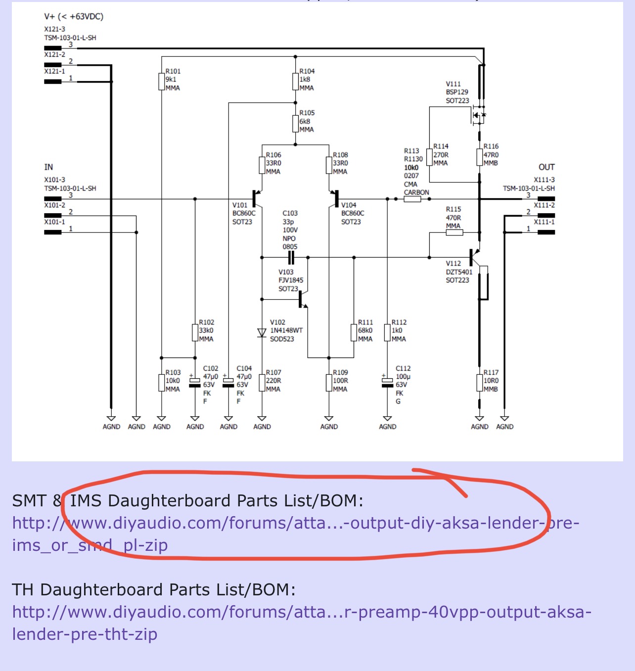
http://www.diyaudio.com/forums/atta...-output-diy-aksa-lender-pre-ims_or_smd_pl-zip
- Home
- Group Buys
- AKSA's Lender Preamp with 40Vpp Ouput GB