The connector signals are series terminated with a resistor, the u.Fl is not.
Btw, what about I2C pull-ups?
Btw, what about I2C pull-ups?
The connector signals are series terminated with a resistor, the u.Fl is not.
Btw, what about I2C pull-ups?
Like Wikipedia writes: "The male connectors are surface-mounted and soldered directly to the printed circuit board. They are designed to have an impedance of 50 ohms." So I am not sure what that means... The U.FL connector has a real 50 Ohm impedance or not???
Pull-up resistors will be placed at the Arduino board (bad idea?), but his is another project... To try will be the parallel mode perfect, or?
Last edited:
Transmission line impedance and termination goes together. The main reason for termination is to compensate for impedance mismatch and suppress resulting signal reflections which cause increased jitter and bad signal quality. As this board is double layer only your line impedance isn't near 50R at all at this trace width.
An easy tool for calculations is the Saturn PCB-Toolkit:
https://www.saturnpcb.com/pcb_toolkit.htm
For the local decoupling caps, get then as close as possible to the chip and disable the thermals for them.
An easy tool for calculations is the Saturn PCB-Toolkit:
https://www.saturnpcb.com/pcb_toolkit.htm
For the local decoupling caps, get then as close as possible to the chip and disable the thermals for them.
I do not really understand what you are writing, I must study-up in this theme. Or you should write me a german text...🙂
Ok, thermals can be disabled by smd-s.
More nearer I can not place them, 1-2mm does not mean anything anyway...
And what about the added red earthing connections?
Ok, thermals can be disabled by smd-s.
More nearer I can not place them, 1-2mm does not mean anything anyway...
And what about the added red earthing connections?
Widerstand gegen Reflexion! - Mikrocontroller.net
fortfolgend
1-2mm means 1-2nH inductance.
For the red grounding, draw the full power patch from the cap to the IC. This means Cap+ -> IC Pin+ -> IC GND -> Cap- ...
You want to have the smallest loop (minimized loop area within the loop) with least inductance.
If you can't put these caps in parallel to the 2 pins, the positive side should always face to the IC, like actually done.
How come you only have one oscillator? Do you intend to only use one "family" of sampling rates?
This was designed to work with ADAU1452 with built in ASRC.
I need to add terminating resistors and a clock buffer IC because now it feeds directly two IC's from the clock.
I need to add terminating resistors and a clock buffer IC because now it feeds directly two IC's from the clock.
Super...🙂
Can I know something else about your design? I have a lot of question....
Schematic maybe?
What OPAs do you use?
You have planed only unbalanced outputs or?
I see the clock and and TVDD regulator (what type?) but for the analog side nothing....
You are using the internal 1,8V LDO or?
How do you connect the control pins? Under the IC are some vias?
2 or 4 sided pcbs?
...
Last edited:
This was designed to work with ADAU1452 with built in ASRC.
I need to add terminating resistors and a clock buffer IC because now it feeds directly two IC's from the clock.
I see. Which one is the second IC?
Super...🙂
Can I know something else about your design? I have a lot of question....
Schematic maybe?
What OPAs do you use?
You have planed only unbalanced outputs or?
I see the clock and and TVDD regulator (what type?) but for the analog side nothing....
You are using the internal 1,8V LDO or?
How do you connect the control pins? Under the IC are some vias?
2 or 4 sided pcbs?
...
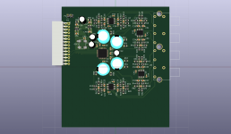
OPA NE5532 or any dual. Only unbalanced.
Electrolytic bypass also missing on OPAMP's.
TVDD and clock regulator LP5907. LT3042 x 2 will be used for analog supply and VREF. Internal regulator is enabled.
TPS7A3301 and TPS7A4701 for OPAMP's.
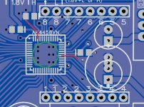
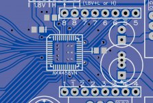
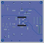
This is a 4 layer PCB. Control pins (I2C, PDN) will go an on a 4 pin header. Serial control mode.
I will upload schematic as soon as I can and pics of the PCB layers.
Last edited:
I see. Which one is the second IC?
I was thinking of CDCLVC1102 for clock buffer.
By the second IC I mean the DSP one.
Last edited:
Thanks!
The other (analog) regulators will be placed on the pcb too if I understand it right?
My design goals are a little different:
2 layer pcb with balanced outputs and fully-differential opas.
For the alanog sides option for shunt regulators.
Regarding master clock I am not quiet sure yet...
(I have at the monent a MiniDSP USBStreamer and it operates only in master mode, so I does not have any sense to place another clock near the DAC)
Last edited:
I was thinking of CDCLVC1102 for clock buffer.
By the second IC I mean the DSP one.
I like this CDCLVC1102. Have you considered the Potato Semi alternative (PO74G38072A)?
Thanks!
The other (analog) regulators will be placed on the pcb too if I understand it right?
My design goals are a little different:
2 layer pcb with balanced outputs and fully-differential opas.
For the alanog sides option for shunt regulators.
Regarding master clock I am not quiet sure yet...
(I have at the monent a MiniDSP USBStreamer and it operates only in master mode, so I does not have any sense to place another clock near the DAC)
Yes all regulators onboard. I don't think that there will be any difference with external regulator for VDD18.
You should try to make this an a 4 layer PCB. It's not difficult and the price difference is small. Mine is 10cm x 10cm.
I like this CDCLVC1102. Have you considered the Potato Semi alternative (PO74G38072A)?
Nothing is final yet.
This project started just for fun. I ran out of time and money.
I need to build a baking oven also.
- Home
- Source & Line
- Digital Line Level
- AK4458 multichannel DAC with I2S input