Hey guys, I'm not sure if a "want ad" is allowed in this section, but I figured most of you probably don't make it to the general FS section so I thought I would risk the wrath of the Mods and ask here. If this is not allowed, I apologize in advance, I will be happy to repost elsewhere if need be.
This isn't strictly a "wanted" post, but I am looking for a DLM4500, revision 3 or 4. The board does not have to be working, in fact I prefer one that you have lost hope in.
Here is the deal, I decided a while back when I took my bad driver board apart for pictures for another guy that it might not be to bad to reverse engineer this thing. I have started with the bad board from my Autotek MX1500.1 and am making progress, however, I found what I suspect is the problem with my board and I would really like to reassemble and test in my amp. I'm leery to keep pulling this board to continue mapping it and drawing it in eagle.
When/If I finish this, I will post up the completed files. With any luck I may even be able to cut replacement boards with my CNC Bridgeport mill... That is the hope anyhow.
So, what have you got? I don't want to spend a ton of money, but I will happily buy a complete blown amp if the price is right.
Thank you all!
Jason
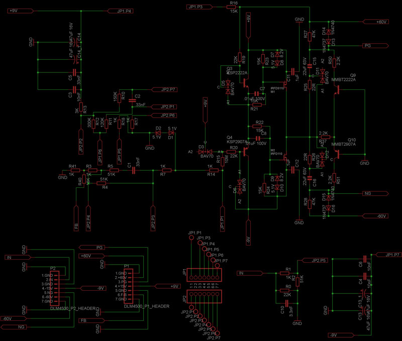
Well, since no one volunteered (I know, I didn't give you all long, no sweat 🙂 ) I decided to just strip my board completely and get some good scans of it to eliminate all the guesswork on where the traces go. I'm just going to put some pin header sockets in my amp and that way I can easily test these if I try to duplicate it. Anyhow, I have a list of every component that I still need to throw into a spreadsheet. I also have a partial schematic in Eagle, but I won't be posting that until I think I am at least close to done. Hopefully some of the smarter minds here and double check things for us 😀
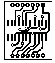
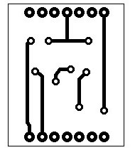
Anyhow, low res copies of the scans are inline below. Linked versions to high res versions are in the "clicky". I'll try to get the BOM in a spreadsheet tonight and post that as well.
I do have a question, I tracked down all the SMD parts on the board, however the only one that I have had trouble identifying with 100% certainty is the diodes in the SOT-23 that are marked KJJ. Cross reference tuned up a BAV70 diode, however, something like 99% of those are marked A4, not KJJ. I found one quite old datasheet, i believe from diodes inc, that showed their BAV70 diodes labeled as KJJ. The BAV70 is the ONLY diode I can seem to find that ever had these markings. There are other SOT-23 parts that had KJJ or JJ, but they are all transistors, and the board clearly marks these as diodes. Anyhow, just wondering if anyone knows with certainty what the SOT-23's marked KJJ are?
Without further ado, here are the pics so far:
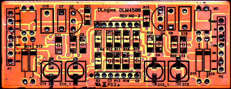
Front high contrast high resolution Clicky.
Front high resolution Clicky.
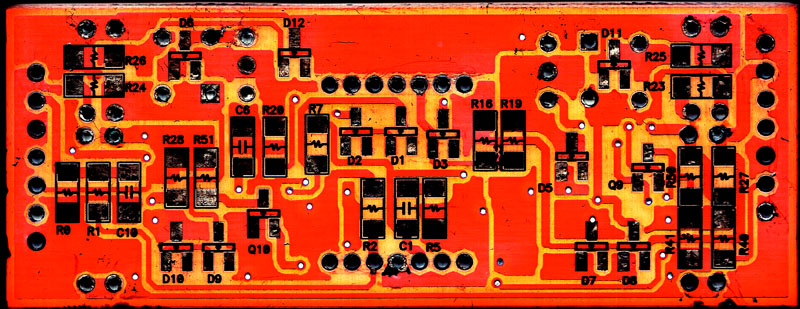
Back high contrast high resolution Clicky.
Back high resolution Clicky.
More later,
Jason
Anyhow, low res copies of the scans are inline below. Linked versions to high res versions are in the "clicky". I'll try to get the BOM in a spreadsheet tonight and post that as well.
I do have a question, I tracked down all the SMD parts on the board, however the only one that I have had trouble identifying with 100% certainty is the diodes in the SOT-23 that are marked KJJ. Cross reference tuned up a BAV70 diode, however, something like 99% of those are marked A4, not KJJ. I found one quite old datasheet, i believe from diodes inc, that showed their BAV70 diodes labeled as KJJ. The BAV70 is the ONLY diode I can seem to find that ever had these markings. There are other SOT-23 parts that had KJJ or JJ, but they are all transistors, and the board clearly marks these as diodes. Anyhow, just wondering if anyone knows with certainty what the SOT-23's marked KJJ are?
Without further ado, here are the pics so far:
Front high contrast high resolution Clicky.
Front high resolution Clicky.
Back high contrast high resolution Clicky.
Back high resolution Clicky.
More later,
Jason
The BAV70 should work. Have you checked to conform that the KJJ has 2 diodes in the configuration shown in the datasheet?
You know Perry, I'm pretty sure I did, but it was like a week ago when I ordered some parts. For some reason I came to the conclusion that they were for sure the correct part, but then today a started second guessing myself. I think I still have the old kjj around, I'll double check them tomorrow.
Thanks,
Jason
Thanks,
Jason
Made a little progress tonight. I planned to get further, but probably won't have any more free time tonight. Attached below is as complete of a BOM as I have been able to make so far. I just now realized I forgot the pin headers... I will add them later. Anyhow, the SMD caps were based on measured values. I am not sure what voltage rating they were supposed to be, but 63V is the highest rated marked cap, so I went with 100V ceramics. I will update as I determine more.
Spreadsheet is in OpenOffice .ODS format. Should be able to open in MS Excel without any trouble.
Clicky for DLM4500 BOM
Later,
Jason
Spreadsheet is in OpenOffice .ODS format. Should be able to open in MS Excel without any trouble.
Clicky for DLM4500 BOM
Later,
Jason
Well, I thought I was going to have schematics for the main board done tonight but instead I am just frustrated. My laptop just froze up when I was probably 10% away from done. Of course it had been a few hours since I saved it... I just had to say screw it. I was going to make mistakes if I went back to it tonight. To make matters worse I have been marking off every trace on some printouts of the scans and now I am not 100% sure how far back I have to go and some of the traces are pretty convoluted. I'm sure I can do it again, I think it opens me up for a greater window of error though unfortunately.
At least I have the factory board layout scans. That should help spot any glaringly obvious errors when I try to do board layout. What a ******** downer though... Almost makes me question my sanity for attempting this in the first place.
I'll try to get back on it tomorrow.
Later,
Jason
At least I have the factory board layout scans. That should help spot any glaringly obvious errors when I try to do board layout. What a ******** downer though... Almost makes me question my sanity for attempting this in the first place.
I'll try to get back on it tomorrow.
Later,
Jason
Well, I finished the main board tonight, it is messy but I think complete. I will clean it up and beautify it another time if I get time. It will probably never look like a pro drawing, I am just a hobbyist and know just enough to be dangerous! Exports are below. Please give me feedback if it looks like I missed anything or screwed anything up.
I also found that I screwed up the link to the BOM and since I cannot edit my post for whatever reason, I will repost a link in this reply.
New BOM link Clicky
Image export of schematic:
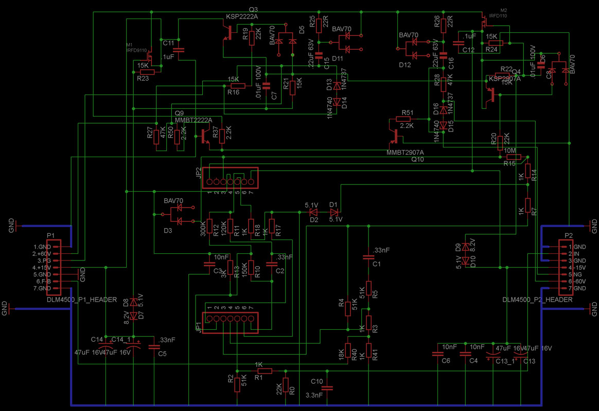
Higher Res version of schematic: Clicky
Later,
Jason
I also found that I screwed up the link to the BOM and since I cannot edit my post for whatever reason, I will repost a link in this reply.
New BOM link Clicky
Image export of schematic:
Higher Res version of schematic: Clicky
Later,
Jason
Oh, I forgot to mention, none of the "KJJ" parts were used as double diodes, only one of the pair was used in each instance that it showed up on the board. It was always pin 1 and 3. I'm going to go out on a limb and guess that the BAV70 is not really the correct part, it seems more likely that it was a single diode in SOT-23 package, just like all the zeners that are scattered throughout. I'm going to try to do some more research and see if I can find a more suitable device, I am guessing the BAV70 is fine from a breakdown voltage standpoint, however this dual diode package is rated at like 200mA. I am not sure, but am thinking that a single diode in the SOT-23 package is probably capable of handling more current. I will try to investigate tonight.
Thanks,
Jason
Thanks,
Jason
I still have not had a chance to check Perry. I got suckered into working 10 midnights in a row after I told you I was going to check last time. I work 12s and live an hour from work, so I literally sleep-drive-work when I am on shift. 10 in a row really sucks, but I'm off on Friday. Hopefully then I can find out for sure.
Another part I am not 100% sure of is C5. I think it is a decoupling cap for the 15V rail supply, just like C6 is for the -15V rail. I suspect it is supposed to be the same as C6, I have one of these SMD caps that I cracked and was still able to measure. I think I wrote down somewhere which one was suspect, this may be it. I don't know how much time I will have to mess with this project tonight. It looks like work is going to be fairly busy.
Thanks,
Jason
Last edited:
Well, the DLM board is labeled +/-15V even though my experience is that every amp that uses this has a +/-9V supply for the DLM board. That said, my sample size is admittedly small, so I was labeling it like the manufacturer did.
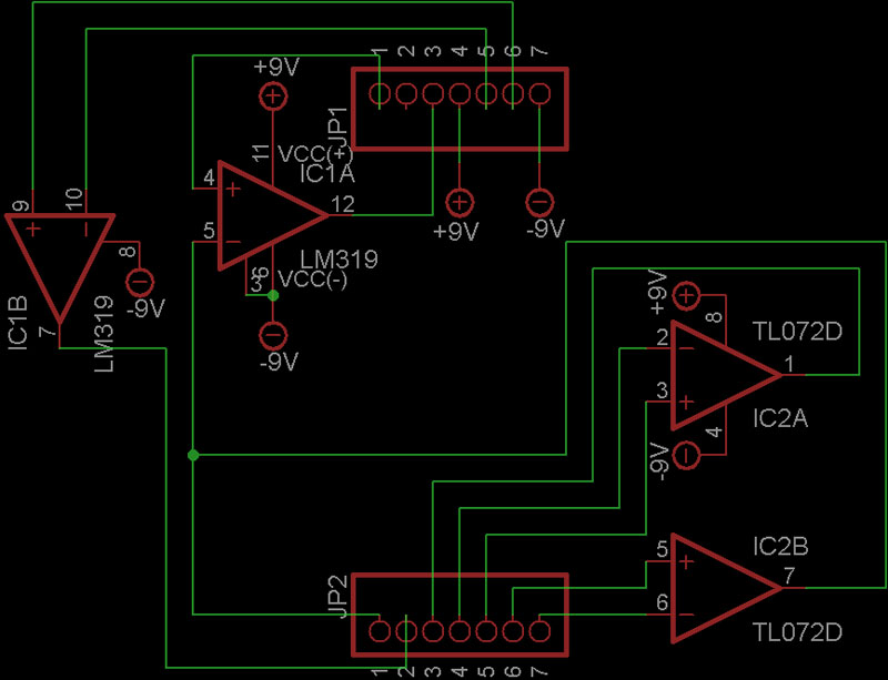
I have been steadily plugging away at this. I reorganized the main schematic. It should be a bit more readable now. Sorry for all the supply/pin designation flags. This was the only way I could think of to do it and keep the nets in tact so that I can do a board layout when I get around to it. I did find a few errors as I was going back through it, so it was a good double check anyhow. I also drew the daughter board, not much there really, and I may make a copy of this with the daughter board included in the main schematic and just eliminate all the header symbols in that version and just use it for reference and not for layout.
Anyhow, I am sure there are more mistakes still, so if you spot something out of the ordinary, let me know and I will double check.
Full Size Clicky
Later,
Jason
Anyhow, I am sure there are more mistakes still, so if you spot something out of the ordinary, let me know and I will double check.
An externally hosted image should be here but it was not working when we last tested it.
Full Size Clicky
An externally hosted image should be here but it was not working when we last tested it.
Later,
Jason
Don't trust this to one file. Copy the file and save it with an altered name if you haven't done so. Emailing it to yourself is additional insurance that it cannot be corrupted or otherwise lost.
Thanks Perry, I have backups of the first version on my google Drive and on thumb drive. I'm looking forward to doing board layout soon. Hopefully that will identify any more errors that I may have.
I've got a bit more progress to share. I did the layout for the daughter board. Admittedly it was the easy one, but it was also the one I need at the moment. I have some pulled vias/through hole plating on mine. I'm thinking about etching one on the mill to see if it will get me by, but I will probably just save it for a board house, I have no huge need to get this amp back up and running quickly.
Anyhow, below is the export of the overall layout and then the front and back layer in monochrome with the back layer mirrored in case anyone wants to take a stab at home etching.
Dimensions of the board outline are .65"x.8". I cannot guarantee that the header positions will line up with a stock Dlogixs board, the pitch is correct, but the header to header spacing may be a few thousandths off what the factory board is. It will match the layout of my drive board when I finish it. If anyone tries to make it before I do and there is a problem. LMK and I'll try to address it.
Overall daughter board:
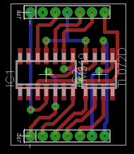
Front side for etching:
Back side mirrored for etching:
More to come later,
Jason
Anyhow, below is the export of the overall layout and then the front and back layer in monochrome with the back layer mirrored in case anyone wants to take a stab at home etching.
Dimensions of the board outline are .65"x.8". I cannot guarantee that the header positions will line up with a stock Dlogixs board, the pitch is correct, but the header to header spacing may be a few thousandths off what the factory board is. It will match the layout of my drive board when I finish it. If anyone tries to make it before I do and there is a problem. LMK and I'll try to address it.
Overall daughter board:
Front side for etching:
Back side mirrored for etching:
More to come later,
Jason
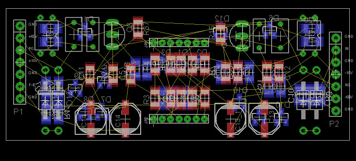
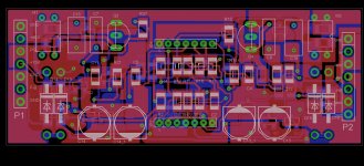
Ok, I have the components all placed on the main board. I still have to do the routing, and I am not looking forward to it. I am probably not going to tackle it tonight, so it will probably be about a week until I get back to this unless I get really, really bored.
Heres a pic for proof 🙂
Later,
Jason
Heres a pic for proof 🙂
Later,
Jason
I finally got the board routed. This little project turned out to be a lot of work! I found several errors in my schematic as I was working on the layout. I will update the schematic pictures when I get some free time. The board still needs some touch-up, I need to adjust spacing on some of the pours and traces, it shouldn't be to bad now. It doesn't look likely that this one will be remotely possible with home etching-- many of the features are just much to close.
On my last days off I did verify that the diodes marked kjj were indeed a dual diode package with common cathode. Also the diodes drop about .6V so it is likely that it is just a plain Jane silicone diode and the BAV70 ought to work ok. Time will tell.
Here is a pic of tonight's progress:

Later,
Jason
On my last days off I did verify that the diodes marked kjj were indeed a dual diode package with common cathode. Also the diodes drop about .6V so it is likely that it is just a plain Jane silicone diode and the BAV70 ought to work ok. Time will tell.
Here is a pic of tonight's progress:
Later,
Jason
Attachments
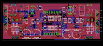
I'm getting closer to done here. I touched everything up tonight. I ran a design rule check based on Oshpark's rules and after a lot of massaging it I got it to pass. I forgot to take a SS of the new schematic and I already put my laptop away for the night. I will get it soon. Below is the overall board layout as well as shots of just the front and back. Please holler if you see anything that looks out of line.
If someone really wants to try to etch these at home, then speak up and I will export them in monochrome with none of the silk screen and you are welcome to try.
Here is where we are at:
If someone really wants to try to etch these at home, then speak up and I will export them in monochrome with none of the silk screen and you are welcome to try.
Here is where we are at:
Attachments


For anyone playing along from home, here is a PDF with both the revised main board schematic and the daughter board schematic. I would recommend not attempting to use the board layouts posted above. I went back through them the other night to make sure the daughter board aligned properly, and I found that I had the vertical spacing of the headers off by a little bit. While I was remeasuring, I found that the high density pin header I used did not match the pin header on the original board. I thought it was a .07" pitch high density header, but after some careful re-checks, it appears it may be 2mm pin spacing. I have ordered a 2mm header and will double check when it arrives. I already updated the layouts for the new header, but I want to double check them before I publish it out to you all.
Here is a link to the PDF:
Schematic PDF
Later,
Jason
Here is a link to the PDF:
Schematic PDF
Later,
Jason
- Home
- General Interest
- Car Audio
- Again with the Dlogixs DLM4500