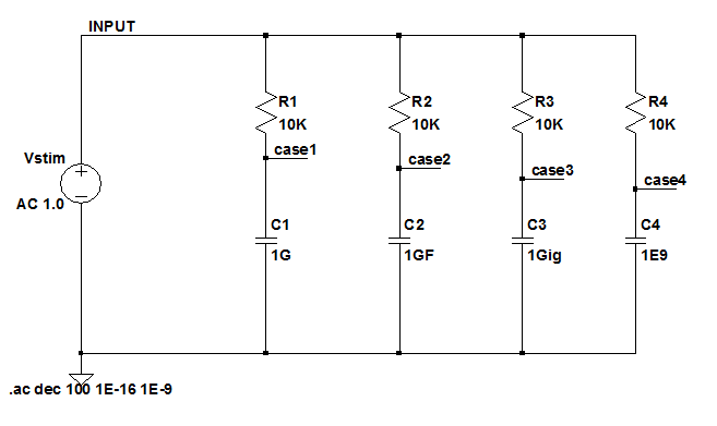
Do we need to type Meg, or Mega, but not meg?
m is *10^-3 but LTspice seems unable to differentiate between M and m
Can LTspice differentiate between k (kilo) and K (Kelvin)?
m is *10^-3 but LTspice seems unable to differentiate between M and m
Can LTspice differentiate between k (kilo) and K (Kelvin)?
Last edited:
One way to find out is to perform a series of experiments.
This figure offers one possible approach; clever experimenters will doubtless invent many others:
_
This figure offers one possible approach; clever experimenters will doubtless invent many others:
_
Level shifting and other issues
Let’s place the stability analysis to one side for the moment… (the Linear Technology/Sennewald approach shows no issues and the Green/Cordell approach seems flawed with LTspice and this situation if only, as was highlighted to me, it shows a voltage potential at the output of the AD797 which exceeds its supply) … and turn back to the DC level shifter and a couple of other items.
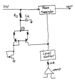
See the circuit in attachment 1. I understand D5, R3, Q1, R1, D6 and C1 as follows. Please correct me if I am wrong.
It might be convenient if the voltage reference for level shifting is the same component type that is used to set the reference voltage for lower Vout versions of the circuit for economies of purchasing. For now I just dropped in a LT1634-2.5 voltage reference.
That would be great if it all worked perfectly. It would reduce dropout voltage by the amount the op amp can’t approach its supply, assuming the voltage reference is high enough. It seems from looking at the TL071 data sheet (fig 10) that 2.5V should be more than enough headroom to deal with this issue. (For now I have only looked at the circuit with the TL071.) That would leave dropout voltage being, roughly, the drop over R2, circa 1-1.1V, and the Vgs of the Mosfet required to deliver the load current, c2.5V.
However, if I look at noise rejection for varying levels of Vin it seems good noise rejection still requires circa 5V of headroom (attachment 2; Vin stepped 16v, 16.5v, 17v, 18v). While there is a marked difference in the current through the LT1634 for 16v versus 16.5v both are well within the operating current of the device. So I don’t understand what’s going on here and where the loss in noise rejection is coming from.
Mark has alluded to the option of replacing the LT1634 with something like a TL431 (or equivalent). If still driven from Vin, it’s reference level would be independent of Vout (although in part responsible for determining Vout). The same could be done with the reference level for the op amp Vref. However, Mark alluded here that such "would be a negative feedback minor loop contained within a positive feedback major loop: bleah!" How can this be a problem if the input to the TL431 is not dependent on Vout? Of course if the ref pin of the TL431 was driven from Vout then that would be a big problem (not dissimilar to my issues with the LT1084/TL431).
Let’s place the stability analysis to one side for the moment… (the Linear Technology/Sennewald approach shows no issues and the Green/Cordell approach seems flawed with LTspice and this situation if only, as was highlighted to me, it shows a voltage potential at the output of the AD797 which exceeds its supply) … and turn back to the DC level shifter and a couple of other items.
See the circuit in attachment 1. I understand D5, R3, Q1, R1, D6 and C1 as follows. Please correct me if I am wrong.
- In overview, there’s a current source endeavouring to provide constant current to the shunt voltage reference such that the op amp’s output is stepped a constant 2.5V under all circumstances while C1 allows the AC variance in voltage to pass directly to the MOSFET
- Presumably the op amp must sink this current
- Because Q1 is biased from Vin the level of current is dependent on Vin (while Q1 does its best to eliminate small signal changes in current as Vin varies with ripple)
- The values of R1 and R3 have to be selected such that the current through the LM4040 stays within its (rather wide) operating current range for all possible levels of Vin
It might be convenient if the voltage reference for level shifting is the same component type that is used to set the reference voltage for lower Vout versions of the circuit for economies of purchasing. For now I just dropped in a LT1634-2.5 voltage reference.
That would be great if it all worked perfectly. It would reduce dropout voltage by the amount the op amp can’t approach its supply, assuming the voltage reference is high enough. It seems from looking at the TL071 data sheet (fig 10) that 2.5V should be more than enough headroom to deal with this issue. (For now I have only looked at the circuit with the TL071.) That would leave dropout voltage being, roughly, the drop over R2, circa 1-1.1V, and the Vgs of the Mosfet required to deliver the load current, c2.5V.
However, if I look at noise rejection for varying levels of Vin it seems good noise rejection still requires circa 5V of headroom (attachment 2; Vin stepped 16v, 16.5v, 17v, 18v). While there is a marked difference in the current through the LT1634 for 16v versus 16.5v both are well within the operating current of the device. So I don’t understand what’s going on here and where the loss in noise rejection is coming from.
Mark has alluded to the option of replacing the LT1634 with something like a TL431 (or equivalent). If still driven from Vin, it’s reference level would be independent of Vout (although in part responsible for determining Vout). The same could be done with the reference level for the op amp Vref. However, Mark alluded here that such "would be a negative feedback minor loop contained within a positive feedback major loop: bleah!" How can this be a problem if the input to the TL431 is not dependent on Vout? Of course if the ref pin of the TL431 was driven from Vout then that would be a big problem (not dissimilar to my issues with the LT1084/TL431).
Attachments
Get rid of Q1 and all its associated doodads.
Get rid of U2 and C1.
Replace Q1 by an ideal current source from Vin to Vgate, whose value is ABCDEF amperes.
Replace U2 by an ideal voltage source from Vgate to OpampOutput, whose value is WXYZ volts.
Question #1: What effect does WXYZ have upon the open loop Bode plot, if any? What values of WXYZ produce the expected "good" behavior? What values of WXYZ produce unwanted "not so good" behavior? Is there a cutoff value of WXYZ, such that WXYZ > CutoffValue gives good behavior?
Question #2: Does there exist a simpler way to find the WXYZ Cutoff, perhaps in a simulation that includes only the opamp and a few ideal sources?
Question #3: What is the WXYZ Cutoff value for opamp A? for opamp B? for opamp C? for opamp D? Does there exist a WXYZ Cutoff design target which allows all four opamps to produce the expected "good" behavior?
Question #4: Does there exist a simple way to answer Question #3, perhaps in a simulation that includes only the opamp and a few ideal sources?
Question #5: Are you worried that all of the above might change, if you select a different value of the current ABCDEF? Why or why not?
Last edited:
Thanks for suggesting using ideal sources to narrow down issues.
I'm still looking at this but it's already clear that setting the level of the dc shift such that the op amp output is closer to mid supply makes sense. While greater levels of Vin are generally good for noise rejection, especially in higher frequencies, raising Vshift to 5-7V allows Vdrop to fall to c2V while still maintaining generally the same noise rejection profile.
Replacing the ideal voltage source with a LT1634-5 leaves the noise rejection profile unchanged. So the issue is the current supply. Varying the ideal current supply across a relatively wide range doesn't change the noise rejection plot. The problem comes when a less than ideal current source (e.g. a JFET with source resistor) replaces the ideal current source.
There's a good chance you are seeing the fact that a real current source needs some voltage across it before it behaves well. JFETs are particularly bad, that's why I apply 5 volts (!) across the MMBF5460 to make sure it operates as a current source.
In your case, you want to design yourself a current source that starts current-sourcing at very little voltage drop. I think a current mirror is the most likely candidate. Instead of the 4 components in your present current source, the current mirror needs 5 components, see below. Emitter degeneration resistors Rj and Rk are chosen so the I*R drop across them is approx 10*(kT/q), namely, 250 millivolts. The input current is 13mA, from a JFET with lots of voltage across it. Lower input voltage regulators could use an LM334 or invent a third idea.
You could put this into a .DC analysis on SPICE and see how close the output collector gets to the input rail before current source behavior stops. Compare to a JFET, cowabunga.
Take a look at (this old post) in which I recommended (a) only 35mV across the emitter degeneration resistors; ameliorated by (b) some truly excellent, low-VCE devices. For your PNP uses, the BC327-40 (datasheet)
_
Attachments
Last edited:
Why don't you post your .asc? IP issues or else?Thanks for suggesting using ideal sources to narrow down issues.
I'm still looking at this but it's already clear that setting the level of the dc shift such that the op amp output is closer to mid supply makes sense. While greater levels of Vin are generally good for noise rejection, especially in higher frequencies, raising Vshift to 5-7V allows Vdrop to fall to c2V while still maintaining generally the same noise rejection profile.
Replacing the ideal voltage source with a LT1634-5 leaves the noise rejection profile unchanged. So the issue is the current supply. Varying the ideal current supply across a relatively wide range doesn't change the noise rejection plot. The problem comes when a less than ideal current source (e.g. a JFET with source resistor) replaces the ideal current source.
If you did, I think the issue(s) could be resolved much more quickly.
Further to the above, when you want a very low-VCE current source, you must select a transistor whose Ice-Vce curves are completely free of QuasiSaturation misbehavior.
In the regime where you are likely to be operating (I_current_source <= 50 mA), I think the following transistor types may be suitable. These recommendations are based upon curve tracer experiments I performed myself, over only two or three samples of each xitor type. Do I remember which mfr made them and which distributor sold them? Sorry, no. Readers with enormous curiosity can replicate my experiments themselves, by purchasing inexpensive test equipment like the Peak DCA Pro (LINK) to run their own curve tracing experiments.
Recommended (very little QuasiSaturation behavior)
NOT Recommended (too much QuasiSat)
In the regime where you are likely to be operating (I_current_source <= 50 mA), I think the following transistor types may be suitable. These recommendations are based upon curve tracer experiments I performed myself, over only two or three samples of each xitor type. Do I remember which mfr made them and which distributor sold them? Sorry, no. Readers with enormous curiosity can replicate my experiments themselves, by purchasing inexpensive test equipment like the Peak DCA Pro (LINK) to run their own curve tracing experiments.
Recommended (very little QuasiSaturation behavior)
- BC337-40 (NPN) + BC327-40 (PNP)
- 2N4401 + 2N4403
- 2N2222A + 2N2907A
- BD139 + BD140
- 2SD882 + 2SB772
NOT Recommended (too much QuasiSat)
- MPSA42 + MPSA92
- 2N5551 + 2N5401
- BC550 + BC560
- KSC1845 + KSA992
- 2N5210 + 2N4250
- 2N5089 + 2N5087
- 2N3904 + 2N3906
Thanks
Okay, I figured out the larger issue I was grappling with. As noted earlier, with a ideal current source Vin can fall to around Vout+2V and still yield good noise rejection. But this is highly misleading. With Vout=12V and Vin=14 an ideal current source still allows Vgate to rise to the required 14.75V - above Vin. Of course, with a more realistic current source the voltage potential at collector of Q3 is Vin less the drop over the emitter resistor. Vdrop is therefore necessarily higher, about 1.25V or so higher. Still, that's around 2.5V lower Vdrop than without the shifter.
That said, even with Vin=15.5V, the addition of the level shifter and its current supply knocks about 10dB off the peak noise rejection which for the TL071 circuit is 130dB @ 82Hz (with shifter). The output at Vin=15.5V is basically the same as the blue line in the second attachment to post 64 and it doesn't improve with greater Vin (except in very high frequencies). Probably still worth the lower dissipation across the pass transistor.
Maybe that can be improved with a better replacement for the LT1634. I'm reticent to dive into TL431/SPX431 type solutions until I'm confident I don't get caught in compounding regulators again. Hence my earlier question in post 64.
Actually I have not used .dc analysis before. I will look at it in the morning. In hindsight, this should have been a very good clue to saving me an hour or so this evening.
(Elvee, I will try to post a version of this TL071 circuit tomorrow. I've had enough for this evening and have also got stuff spread between home and office. I really shouldn't be spending so much time on this at the latter!)
Okay, I figured out the larger issue I was grappling with. As noted earlier, with a ideal current source Vin can fall to around Vout+2V and still yield good noise rejection. But this is highly misleading. With Vout=12V and Vin=14 an ideal current source still allows Vgate to rise to the required 14.75V - above Vin. Of course, with a more realistic current source the voltage potential at collector of Q3 is Vin less the drop over the emitter resistor. Vdrop is therefore necessarily higher, about 1.25V or so higher. Still, that's around 2.5V lower Vdrop than without the shifter.
That said, even with Vin=15.5V, the addition of the level shifter and its current supply knocks about 10dB off the peak noise rejection which for the TL071 circuit is 130dB @ 82Hz (with shifter). The output at Vin=15.5V is basically the same as the blue line in the second attachment to post 64 and it doesn't improve with greater Vin (except in very high frequencies). Probably still worth the lower dissipation across the pass transistor.
Maybe that can be improved with a better replacement for the LT1634. I'm reticent to dive into TL431/SPX431 type solutions until I'm confident I don't get caught in compounding regulators again. Hence my earlier question in post 64.
You could put this into a .DC analysis on SPICE and see how close the output collector gets to the input rail before current source behavior stops. Compare to a JFET, cowabunga.
Actually I have not used .dc analysis before. I will look at it in the morning. In hindsight, this should have been a very good clue to saving me an hour or so this evening.
(Elvee, I will try to post a version of this TL071 circuit tomorrow. I've had enough for this evening and have also got stuff spread between home and office. I really shouldn't be spending so much time on this at the latter!)
Last edited:
Circuit A (no level shifter) has no connection whatsoever, between Vin and the pass transistor gate. The impedance of the path from Vin to pass transistor gate, is Infinity ohms.
Circuit B (current source + level shifter) inserts a BJT and resistor in a direct path from Vin to the pass transistor gate. The impedance of the path from Vin to pass transistor gate is (the output impedance of the current source, about 0.5 megohms). Are you actually surprised that circuit B conducts more AC signal from Vin to the pass transistor output?
If -130dB (do the math: that's 0.3 parts per million) of input ripple rejection at 82Hz is insufficient, there are options. They add design time, design complexity, parts cost, and board area. But they do exist and they will increase ripple rejection at 82Hz. And they are additive, if you choose to implement more than one.
- RC filter the current source's more positive node ("T"); arrange for this filter to attenuate (oh let's just say) -10dB at 82 Hz. This means Rj*Ck > 23 milliseconds. You probably don't want to drop more than 100 millivolts across Rj; with a total of 30mA flowing in the two BJTs, that means Rj < 3.3 ohms. Thus Ck > 6900 microfarads. Although a capacitor this big is expensive and cumbersome, it won't noticeably lengthen the wakeup time of the regulator at power-on. You've got other things going on at power-on which require much more than 0.023 seconds to complete.
- Cascode the current source. Adds another ~ 200mV of drop across the current source, increases its output impedance by ~ 20X (26dB)
- Give up on ever building a negative voltage regulator; use a depletion mode MOSFET pass transistor (they are only available in Nchannel). Now Vgate is less than Vout, about -1V less. Many opamps will be able to drive this output voltage directly, without a level shifter, especially if you also do the next stunt:
- Change the opamp's positive supply rail filter network so that less than 150 millivolts are dropped across the series resistor. Every millivolt dropped across this resistor is a millivolt robbed from the output pin, is a millivolt MORE level shift you require. While you're at that node, increase the RC timeconstant of the filter. Currently it's 71 milliseconds. Triple that, thereby adding 9.5dB to the opamp's PSRR at 82 Hz. Yes the capacitor is big and expensive but at least you're not injuring the wakeup time at power on.
- Use a high-beta, high-fT, bipolar as a pass transistor. Now Vbase is only 0.7 volts above Vout, instead of 2 or 3 volts with a MOSFET. You might not need a level shifter. Today's best choice may well be the 2SC5171. Good fT, good beta, mediocre max power dissipation (20W) because it's in a plastic, isolated-case TO220.
Attachments
Are you actually surprised that circuit B conducts more AC signal from Vin to the pass transistor output?
No, not at all. It always seemed to me that a deficiency of the BJT pass transistor was the dependency on the Vin to base connection. (And that shifting the Vs of the op amp to Vout was undermined by this.)
If -130dB (do the math: that's 0.3 parts per million) of input ripple rejection at 82Hz is insufficient, there are options.
It is fine (I now have a better sense of perspective here) but, of course the real target is the AD797-based circuit. I was merely seeking to avoid the green line in post #64. The value of the level shift is with respect to SOA of the pass transistor. Vds of 6V or so and 5A peak is right close to the DC limit of SOA.
Thanks for the list, it is good to understand options and permutations - and more importantly why they make a difference. Your current mirror was immediately recognisable from 'The Art of Electronics' textbook, albeit with the JFET replacing their resistor, and the discussion there was useful. The example that follows that one is a Wilson Mirror.
On your list, perhaps a couple of questions/comments:
- RC filter the current source's more positive node ("T"); arrange for this filter to attenuate (oh let's just say) -10dB at 82 Hz. This means Rj*Ck > 23 milliseconds.
- Change the opamp's positive supply rail filter network so that less than 150 millivolts are dropped across the series resistor. Every millivolt dropped across this resistor is a millivolt robbed from the output pin, is a millivolt MORE level shift you require. While you're at that node, increase the RC timeconstant of the filter. Currently it's 71 milliseconds. Triple that, thereby adding 9.5dB to the opamp's PSRR at 82 Hz. Yes the capacitor is big and expensive but at least you're not injuring the wakeup time at power on.
I had intended to do the second of these, at a minimum lowering the resistor to 100 ohms. Please help me with the maths. I understand that enlarging the capacitor pushes the fc of the low pass filter lower (from c2.25Hz to 0.75Hz) thereby improving filtering and increasing PSRR at any given frequency as the 20dB per decade roll-off shifts left but I'm sure the maths (dB benefit at Hz X) is a lot simpler than what I just attempted on paper... And I am completely missing the time domain perspective here...
Helmut Sennewald came back to me with respect to the stability analysis - both his/LT's method and Cordell/Green's. I post regarding this when I get a chance. Of course, as my luck would surely have it, the injected voltage source was shifted to the last plausible option...
PS: The commercially available TL071-based reg I've mentioned before seems to have a 47k resistor from op amp output to ground. I'm puzzled as to the point of this. (Note it doesn't have level shift and related current source.)
Last edited:
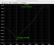
Returning to stability with the AD797
See attached two images. The first shows the two loop gain test circuits: at the top is the Cordell/Green method and below it the Sennewald/Linear Technology method. Note two changes to the first and one to the latter made by Helmut:
1. Size of inductor and capacitor associated with the AC injection to 1Meg and 10F, respectively. Still both large. The alteration to the inductor was likely unnecessary but the change in capacitor makes a difference.
2. The large 10F capacitor placed from Vref to ground. I've asked Helmut why this is necessary/appropriate.
3. AC insertion point for the Sennewald/Linear Tech approach shifted to the one spot I didn't try. 🙁 This makes a difference in the lower frequencies.
The second chart shows the output. Importantly, note that -V(x)/V(vnfb) is plotted for the Cordell/Green approach and -V(Vout)/V👍 for the Sennewald/LT approach. As Mark has noted previously, with the former method, if the amplitude of the injected AC signal is one then -V(x)/V(vnfb) collapses to -V(x). The minus sign doesn't change AolB but it is important for phase. Tim Green's tutorial calculates AOL and 1/B separately and while I follow the collapse of his equations for these so as to produce a plot of AolB directly, clearly I have missed something with respect to phase which means the minus sign is important. I'm sure Mark has the answer.
After all of that, see that the two methods (with the respective changes) overlap each other for all but the very highest frequencies. At AolB=1 (0dB) phase margin is about 55 degrees. There's 27dB of gain margin at phase = -180 degrees. All good. Phew! (Now I am sure it will all go up in smoke when I insert the DC shift into this circuit!)
Attachments

The math is pretty simple but the calculations are involved. If you haven't done them five thousand times with pencil and paper in your EE undergrad homework, you may not have a "feel" for what the right answer ought to be, and a teeny slip can easily cause a two-orders-of-magnitude error. Far more reliable to just go to the computer and build a little 3 element SPICE simulation: Vsource, R, C and then vary R or C as appropriate for your circuit. If SPICE is correct (and it is), you'll get the right answer on the first try even if you have no "feel" for it. If SPICE is not correct, much of Silicon Valley comes crashing down in flaming rubble.
Here's the math for a single-R, single-C, lowpass filter:
Here's the math for a single-R, single-C, lowpass filter:
Transfer function "H(jw)" = Vout/Vin = 1/(1 + 2*pi*f*R*C*j)
where j = sqrt(-1) = the unit of imaginary numbers.
Magnitude of (Vout/Vin) = sqrt( 1 / (1 + (2*pi*f*R*C)^2) ) . . . . {after a lot of algebra}
If 2*pi*f*R*C << 1 (i.e. at low frequencies, below the lowpass cutoff), the first term in the denominator greatly exceeds the second term in the denominator. So it is safe to ignore the second term in the denominator and the magnitude of (Vout/Vin) approaches 1. The lowpass filter doesn't attenuate.
If 2*pi*f*R*C >> 1 (i.e. at frequencies above the lowpass cutoff), the second term in the denominator greatly exceeds the first term. So it is safe to ignore the first term in the denominator, the square-root cancels the squared, and the magnitude (Vout/Vin) becomes 1/(2*pi*f*R*C). As frequency rises, magnitude(Vout/Vin) falls (the very definition of a lowpass filter). Frequency f is raised to the first power, so the slope of the fall is 1 decade of magnitude per decade of frequency. i.e. -20dB per decade.
But SPICE is more reliable if these calculations haven't been seared into your skull by countless repetitions.where j = sqrt(-1) = the unit of imaginary numbers.
Magnitude of (Vout/Vin) = sqrt( 1 / (1 + (2*pi*f*R*C)^2) ) . . . . {after a lot of algebra}
If 2*pi*f*R*C << 1 (i.e. at low frequencies, below the lowpass cutoff), the first term in the denominator greatly exceeds the second term in the denominator. So it is safe to ignore the second term in the denominator and the magnitude of (Vout/Vin) approaches 1. The lowpass filter doesn't attenuate.
If 2*pi*f*R*C >> 1 (i.e. at frequencies above the lowpass cutoff), the second term in the denominator greatly exceeds the first term. So it is safe to ignore the first term in the denominator, the square-root cancels the squared, and the magnitude (Vout/Vin) becomes 1/(2*pi*f*R*C). As frequency rises, magnitude(Vout/Vin) falls (the very definition of a lowpass filter). Frequency f is raised to the first power, so the slope of the fall is 1 decade of magnitude per decade of frequency. i.e. -20dB per decade.
Last edited:
Another idea: build a DC-to-DC boost converter to change +15V into +25V, then filter the hell out of the +25V and apply it to the opamp's positive power supply pin. Now the opamp can comfortably pull its output pin to at least +20V.
This gives two benefits
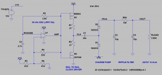
The schematic shows a 50 kHz Schmitt trigger oscillator, followed by a rail to rail clock driver, followed by a capacitor + diode Charge Pump, followed by an RC filter. That's all there is. Really.
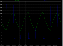
The opamp's input pins can differ by as much as 10 volts during startup, so you don't want a bipolar opamp here. Use a TL081 or other JFET input opamp here, that can tolerate 15 volts of differential input voltage. I've plotted the two input nodes so you can see the Schmitt Trigger action and the truncated exponential (approximating a triangle wave) on the RCNODE.
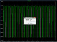
I've attached a plot of current drawn from the +15V supply. The looooong term average current drawn from +15V is 37 mA, and of course there are large current peaks when the clock driver switches.
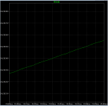
The last plot is the output voltage; vertical magnification is 100 microvolts per gridline. You can see the step height (one step per clock cycle) is teeny tiny; less than 10 microvolts per grid. It's a fairly clean supply but of course you could add more RC filtration to reduce the ripple even more, if desired.
This gives two benefits
- No level shifter is needed
- A standard enhancement mode MOSFET with standard gate threshold voltage of ~ 4.0 volts, can be used as the series pass transistor, and it won't introduce extra dropout voltage.
The schematic shows a 50 kHz Schmitt trigger oscillator, followed by a rail to rail clock driver, followed by a capacitor + diode Charge Pump, followed by an RC filter. That's all there is. Really.
The opamp's input pins can differ by as much as 10 volts during startup, so you don't want a bipolar opamp here. Use a TL081 or other JFET input opamp here, that can tolerate 15 volts of differential input voltage. I've plotted the two input nodes so you can see the Schmitt Trigger action and the truncated exponential (approximating a triangle wave) on the RCNODE.
I've attached a plot of current drawn from the +15V supply. The looooong term average current drawn from +15V is 37 mA, and of course there are large current peaks when the clock driver switches.
The last plot is the output voltage; vertical magnification is 100 microvolts per gridline. You can see the step height (one step per clock cycle) is teeny tiny; less than 10 microvolts per grid. It's a fairly clean supply but of course you could add more RC filtration to reduce the ripple even more, if desired.
Attachments
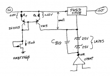
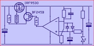
That's a Pchannel common source amplifier in cascade with an opamp. The Pchannel stage's gain and phase will vary with the load current and load impedance, making frequency compensation quite a challenge. You may need to "slug" the HF performance (roll-off prematurely) to get unconditional stability with all loads.Why not doing something likev this ?
No current source , no level shifter 😎
Mona
The schematic drawing contains a small mistake: the opamp's + and - input terminals are reversed. Since the opamp output is connected to the input of an inverting amplifier stage (Pchannel common source amp), the reference diode needs to connect to the opamp's - terminal and the voltage-divided output needs to connect to the + terminal.
- Status
- Not open for further replies.
- Home
- Amplifiers
- Power Supplies
- Adventures with 5A regulated voltage circuits