OK, now put a unity gain buffer (I mean a regular unity gain buffer, look on wikipedia) followed by a pot in front of your circuit and ask the second opamp for a bit more gain. Don't worry too much about the compensation value, just put the pads for a cap. You may not need one. Move the coupling cap and one of the 2M2s to the input, resistor closest to the opamp. Put a cap parallel to it to stop higher frequencies getting into the amp.
Don't draw the feedback network like that, put the cap and resistor pointing down and use another ground symbol.
Try and use decade values and aim for whole number gains, I can do dB's in my head but if you want people to evaluate your work, don't force them to use a calculator. 100k and 10k give you a gain of 11, which is close enough to 10 for all intents and purposes. 20dB.
As bentsnake said, you'll have to think about a power supply. Either dual-rail, or a virtual ground, or redraw the circuit for single rail.
Last edited:
OK, now put a unity gain buffer (I mean a regular unity gain buffer, look on wikipedia) followed by a pot in front of your circuit and ask the second opamp for a bit more gain. Don't worry too much about the compensation value, just put the pads for a cap. You may not need one. Move the coupling cap and one of the 2M2s to the input, resistor closest to the opamp. Put a cap parallel to it to stop higher frequencies getting into the amp.
Put another buffer in front of it? Okay, that's going to be a no go. This has to fit inside a guitar body with a lot of other electronics. I can't be putting multiple buffers in there.
Would it not work just as it is? I'm planning to follow it with a standard passive 10K volume pot.
Don't draw the feedback network like that, put the cap and resistor pointing down and use another ground symbol.
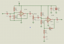
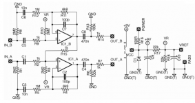
I didn't draw this circuit. It's from the manual for the prefab PCB I'm working from. I just photoshopped it to change some of the values for my purposes.
I just picked the 50K resistor to ground and then chose a feedback resistor that would give 15-20 dB gain and for which it would be possible to find an accurately matched bias resistor (ie. 291K gives 42.7K bias, both available values on mouser). The exact amount of gain isn't that important to me as long as it's all appropriately calibrated and will work.Try and use decade values and aim for whole number gains, I can do dB's in my head but if you want people to evaluate your work, don't force them to use a calculator. 100k and 10k give you a gain of 11, which is close enough to 10 for all intents and purposes. 20dB.
Sorry re: calculators though.
As bentsnake said, you'll have to think about a power supply. Either dual-rail, or a virtual ground, or redraw the circuit for single rail.
The board already comes with pads for single supply. I've attached the full original schematic. I plan on leaving the power portion the way it is.
This is the PCB I'm populating:
An externally hosted image should be here but it was not working when we last tested it.
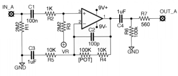
So what do you think. Single noninverting buffer with 17 dB gain, powered by 9V+, followed by 10K volume pot. Overall will the values I suggested likely work, or is there anything obvious I'm still missing?
Attachments

Last edited:
This is what I would do. I wouldn't allow myself to be constrained by the fact that I had a circuit board. Get a scrap of veroboard. It's a dual opamp, so same size. You need this one, fet input
Attachments
Last edited:
This is what I would do. I wouldn't allow myself to be constrained by the fact that I had a circuit board. Get a scrap of veroboard. It's a dual opamp, so same size. You need this one, fet input
I actually plan on using each opamp for a different buffer in the prefab PCB. I've got multiple outputs from the guitar and each needs a buffer, so I'm trying to keep the buffers as simple and compact as possible.
Thank you very much for sharing a design. That's generous of you.
Can I ask why you are suggesting the two opamp stages though? I'm not sure what the shortcoming of the single opamp buffer is. Shouldn't it work just fine the way I posted?
Most guitars with buffers are buffered by a single opamp buffer stage. It tends to work well. I just want to add a small bit of gain, which I think the OPA2134 should be more than capable of providing with the feedback resistor as posted.
Am I still missing something?
.
So variable gain, so sure, so why not variable gain. Combination R5 and R5a can be any values you wish.
Remember that feedback resistor R4, and gain resistor R5, are actually part of the op amp, made exterior to allow adjustment. All you're doing here is changing the value of the gain resistor so there are no issues with other parts of the circuit.
<< ...I just want to add a small bit of gain, which I think the OPA2134 should be more than capable of providing... >>
You've spoken of this more than once. Don't worry, the OPA2134 is an amplifier in the first place. It can provide more gain that you could ever possibly want. The TL072 likewise.
.
Attachments
Last edited:
.
So variable gain, so sure, so why not variable gain. Combination R5 and R5a can be any values you wish.
Remember that feedback resistor R4, and gain resistor R5, are actually part of the op amp, made exterior to allow adjustment. All you're doing here is changing the value of the gain resistor so there are no issues with other parts of the circuit.
.
The only thing I don't get about what you suggested (which is what I was intending to do half way through the thread) is that I had read R2 (the compensating resistor) should be set to the parallel resistance of R4 and R5, as shown here:
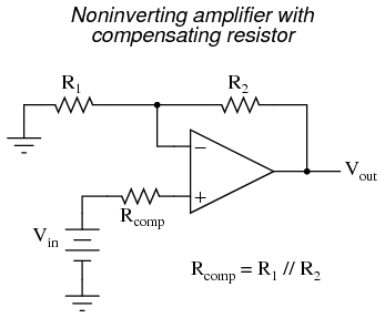
Practical considerations : Operational Amplifiers - Electronics Textbook
The problem would then be a variable feedback resistor would require a variable compensating resistor too to maintain appropriate input bias.
Or is this not necessary to worry about for some reason, like due to the 2M2 resistors? I think I remember reading that once ...
I don't know the answer to your R3 question, but here's the full original PCB schematic if it helps:
Last edited:
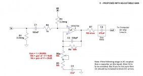
OK, I have juggled the values a bit.
You want to add variable gain. You can't add the attenuator at the input, because it will load down the guitar pickup. In order to prevent that we use the high input impedance buffer which the guitar sees as it's load. Now we can use the comparatively low impedance pot and drive it with the buffer output. This enables us to reduce the output to zero.
I'm keeping the values moderately high here because it means that the caps can be obtained as non-electrolytics. The caps are obviously selected to maintain the kind of bandwidth you require, some are oversize in place, but it keeps the BOM simple. The pot has a minimum impedance of 1/4 of it's end-to-end value. 100k->25k. This dictates the minimum size for the caps.
Now we add the gain stage. Because the supply is single sided, the opamp output is at half the supply voltage. This means that to avoid DC flowing in the pot, we need to isolate it with caps. The second opamp's output is similarly biassed to half-supply with a resistive divider.
So now your output can be driven direct from the second opamp without loading it with a low resistance pot (and accompanying large cap) which will be more robust and versatile and have a constant output impedance, and so will not interact with the next device in line as changes are made to the gain.
The circuit achieves it's goals step-by-step, but this is often necessary to keep out of the clutches of the law of unintended consequences.
Attachments

So now your output can be driven direct from the second opamp without loading it with a low resistance pot (and accompanying large cap) which will be more robust and versatile and have a constant output impedance, and so will not interact with the next device in line as changes are made to the gain.
The circuit achieves it's goals step-by-step, but this is often necessary to keep out of the clutches of the law of unintended consequences.
I see. So the reason you're suggesting it is that using a passive volume pot after the buffer (as most active guitars are designed with) will result in variable output impedance. I'm not sure this is going to be significant to me either way though. The soundcard I have has analog inputs with 10K input impedance. As long as the output of the opamp buffer is lower than that (after travelling through the 10K pot), I should be fine, shouldn't I?
The OPA2134 is 10 ohms max output impedance. I have just read than a volume pot's contribution to impedance is maximum 1/4 its value when at the 50% point (reference), so this would mean my output impedance at 50% volume would be 2.5K maximum. This is still well below the 10K input impedance of the sound card so should work fine I think without compromising the audio quality.
I appreciate the benefits of robustness you're suggesting, as well as the time and energy you put into the schematic you posted, but as long as it will likely work with a single buffer followed by a pot, that would be preferential for me as I just have so much circuitry to pack into such a small space.
Last edited:
.
Just to be picky, it would be correct to say "bias compensation resistor." There are all kinds of compensation showing up all over the place in all kinds of circuits, so it's better to be specific.
Getting to your question, you're right about R2. But here's where using the correct terms comes in. Lecture follows.
For convenience, we pretend that op amps draw no current through their inputs (inverting and non-inverting), but actually they do. It's the very small "bias current" you see listed in the data sheets. "Very small" being in the area of nanoamps (three decimals smaller than microamps) or less.
In the referenced (and most other) circuits this small current flows through whatever resistance is connected between the input and ground. And current flow through a resistor produces...tada...a voltage drop (E=IR). Ground is zero volts by definition, so this voltage appears at the input pin of the op amp.
If the other input pin is connected directly to ground, or to some other voltage, then different voltages appear at the two input pins. This produces an imbalance in the inner working of the op amp, which results in DC errors at the output.
Solution: whatever resistance might be connected to one pin, connect a balancing resistance to the other pin. Bingo, things are in balance and DC errors are minimized. Not eliminated (no errors ever are), but minimized. The balancing resistor in this case is, as you say, R2, the bias compensation resistor
One teensy problem with this great plan is that you can't always do it--for this or that reason you can't always put in a bias compensation resistor. So then what? There are various solutions, some of them pretty complicated, but the usual thing to do is just add a capacitor to the output. Capacitors block DC (they actually block steady-state currents), so the DC errors can't go forward to the following stages. This is commonly done, it's pretty much the main reason you see interstage capacitors.
End of lecture. And now a more succinct answer to your question. You said, "The problem would then be a variable feedback resistor would require a variable compensating resistor too to maintain appropriate input bias."
Well...picky me...don't worry about maintaining appropriate input bias. Either the op amp will draw the bias current it needs, or it won't work. The situation is the need to maintain appropriate bias current compensation.
The answer, to get to it at last, is twofold. First of all you're right, with variable gain you can't have correct bias compensation. End of story.
But second, it doesn't matter. This is because you're using a single-supply circuit, so an output capacitor is mandatory, so DC errors are blocked anyway. Also end of story.
But there's actually a third factor, which is that the bias current of the OPA2134 is very, very small, in the picoamp region, which is three decimals smaller than nanoamps. So even across large resistors the voltage drop is not that much, so the DC error is not that high. The TL072, being also a JFET input op amp, is similar. OK now really end of story.
Except to add that these DC errors are small with the OPA2134 and TL072, but that doesn't mean they don't matter, because they do. You're wise to take them into consideration. Only not in this case.
Thanks for posting the complete schematic. It did clear up the mystery of R3.
.
The only thing I don't get about what you suggested (which is what I was intending to do half way through the thread) is that I had read R2 (the compensating resistor) should be set to the parallel resistance of R4 and R5, as shown...
Just to be picky, it would be correct to say "bias compensation resistor." There are all kinds of compensation showing up all over the place in all kinds of circuits, so it's better to be specific.
Getting to your question, you're right about R2. But here's where using the correct terms comes in. Lecture follows.
For convenience, we pretend that op amps draw no current through their inputs (inverting and non-inverting), but actually they do. It's the very small "bias current" you see listed in the data sheets. "Very small" being in the area of nanoamps (three decimals smaller than microamps) or less.
In the referenced (and most other) circuits this small current flows through whatever resistance is connected between the input and ground. And current flow through a resistor produces...tada...a voltage drop (E=IR). Ground is zero volts by definition, so this voltage appears at the input pin of the op amp.
If the other input pin is connected directly to ground, or to some other voltage, then different voltages appear at the two input pins. This produces an imbalance in the inner working of the op amp, which results in DC errors at the output.
Solution: whatever resistance might be connected to one pin, connect a balancing resistance to the other pin. Bingo, things are in balance and DC errors are minimized. Not eliminated (no errors ever are), but minimized. The balancing resistor in this case is, as you say, R2, the bias compensation resistor
One teensy problem with this great plan is that you can't always do it--for this or that reason you can't always put in a bias compensation resistor. So then what? There are various solutions, some of them pretty complicated, but the usual thing to do is just add a capacitor to the output. Capacitors block DC (they actually block steady-state currents), so the DC errors can't go forward to the following stages. This is commonly done, it's pretty much the main reason you see interstage capacitors.
End of lecture. And now a more succinct answer to your question. You said, "The problem would then be a variable feedback resistor would require a variable compensating resistor too to maintain appropriate input bias."
Well...picky me...don't worry about maintaining appropriate input bias. Either the op amp will draw the bias current it needs, or it won't work. The situation is the need to maintain appropriate bias current compensation.
The answer, to get to it at last, is twofold. First of all you're right, with variable gain you can't have correct bias compensation. End of story.
But second, it doesn't matter. This is because you're using a single-supply circuit, so an output capacitor is mandatory, so DC errors are blocked anyway. Also end of story.
But there's actually a third factor, which is that the bias current of the OPA2134 is very, very small, in the picoamp region, which is three decimals smaller than nanoamps. So even across large resistors the voltage drop is not that much, so the DC error is not that high. The TL072, being also a JFET input op amp, is similar. OK now really end of story.
Except to add that these DC errors are small with the OPA2134 and TL072, but that doesn't mean they don't matter, because they do. You're wise to take them into consideration. Only not in this case.
Thanks for posting the complete schematic. It did clear up the mystery of R3.
.
Last edited:
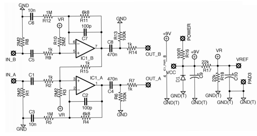
Post40 sch
reduce your resistor values by a factor of ten.
R2= 4k3, R3=220k, R5=5k1, R4=30k
R1=2M2, R6=100k can remain as shown.
I'd suggest a reduction for R7. Try values of 51r upto 220r and use the minimum value that allows good performance, even when some parasitic capacitance is added to the load.
To get this 10 reduction in resistors you need to increase the capacitor C1 by a factor of ten & capacitor C3 by a factor of 100. Cap C2 may have to be reduced substantially
.
I more or less hate to bring it up at this late date, but now that the full schematic has been posted (re-posted below), the power supply seems to contain a curve ball in the form of VR. This is in addition to looking kinda weird in the first place, but that's another story.
If I'm right, VR is a "reference voltage." This relates to the DC errors caused by bias current discussed in post #49.
A reference voltage is another method for dealing with bias current errors. A DC voltage distinct from all others (but taken from the same power supply) is applied to the appropriate input pin. This voltage is measured or calculated to be equal in amplitude to the bias current error, but opposite in polarity. Thus bias current error is cancelled.
This is effective, but also a bit complicated. And as a matter of fact the whole thing is a non-issue in counter culture's circuit (post #47), because his C6, C3, and C4 block DC.
It all depends on what you wind up doing, of course. But in any case the referenced power supply seems to me to be kinda strange. So I thought I'd throw in a brief commercial announcement.
Ummm...I couldn't interest you in a nice dual supply? Available in different colors, depending on what brand of batteries you buy, and on special this week when you present your forum membership card!
You might get the impression that I disapprove of single supplies, and want to wipe them from the face of the earth. Well, they do create problems where there were none before, they do call for additional parts, and therefore they do increase the chances for breakage and error. Sooo, dual supply, so just a thought.
.
Attachments

.
So variable gain, so sure, so why not variable gain. Combination R5 and R5a can be any values you wish.
Remember that feedback resistor R4, and gain resistor R5, are actually part of the op amp, made exterior to allow adjustment. All you're doing here is changing the value of the gain resistor so there are no issues with other parts of the circuit.
Thanks for the explanations and suggestion. You put the potentiometer with R5 to ground. The problem with that is as you vary the potentiometer, it will vary the frequency filter of the C3 capacitor there, no?
I think it makes more sense to put it in the opamp feedback loop, because then you're always still filtering with C3 at a set frequency to ground. ie. 16 hz as attached.
I put the bias compensation resistor back to 1K. I took AndrewT's suggestion also to reduce the resistor values and others' suggestions to reduce the output resistor. This gives me 0-21 dB gain and I think it should be perfectly stable at both extremes.
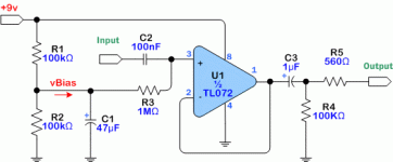
I increased the output capacitor to 1uF with 560 ohms solely because that's what's used in the Klon buffer circuit which is one of the most popular and successful guitar buffers so I figure it generally works in this application (Klon circuit attached for comparison).
Do I need to increase C1? Why? Again this is the same value as used in the Klon and it seems to work well there.
Regarding single vs dual supply, ironically I will actually have a dual supply coming into the guitar as another module I'm installing needs bipolar power. Everything will be running off an external rack mount bipolar PSU I'm building (built it already but unipolar so now I need to change the transformer and regulator to bipolar).
So I COULD run this buffer/amplifier circuit off of bipolar. But it will work fine on unipolar. I already have the prefab buffer PCB's to build it this way. I don't think it's worth the hassle of veroboarding the attached circuitry from scratch just so it can be bipolar. I don't know how much performance improvement I'm going to get for such a simple application from 9V+/- vs. just 9V+.
(Also I know the potentiometer is not drawn or indicated correctly. Like I said, I'm just doing a photoshop here. I think it still should make sense.)
Attachments

Last edited:
You put the potentiometer with R5 to ground. The problem with that is as you vary the potentiometer, it will vary the frequency filter of the C3 capacitor there, no?
Yes, but the variation doesn't matter because C3 is an overkill value. This is commonly done, at least by me. That is...when possible, which it isn't always.
Setting all else aside for a moment, I'm not going to belabor the single/dual power supply issue, but I'm going to add one more comment because it leads into a point I want to make.
All the chips discussed here, and nearly all audio chips used around here, run on dual voltages. That is, they need positive and negative voltages from a power supply to operate. It's impossible to run these chips on a single voltage.
Before your head explodes understand this: The facts are as I've stated above. In the "single supply" case what you do is go through some contortions to create a virtual ground, and by this means create virtual positive and negative voltages that will run the chip. The same positive and negative voltages you'd get from a dual supply in the first place.
All of which is to say that you take the long way around, adding components and complexity, to get to the same place by a more difficult route. Crossing the street by way of Chicago.
Not to say this is bad, just to point it out as a fact. Which leads into the promised point.
The point is as follows: No kidding, it's time, past time, to decide on exactly what power supply you're going to use. I don't mean just single or dual, I mean a specific circuit.
This is mainly because I'm sure you're going to use a single supply, and these are a different kettle of fish. A dual supply is like a battery, you just plug it in anywhere you see plus and minus signs. But single supplies don't work that way, they have to be integrated into the audio circuit (those contortions). If you want to know why read this: http://www.analog.com/static/imported-files/application_notes/AN-581.pdf
Once again proving that the audio circuit hardly matters, it's the power supply that's important.
Please don't think I'm making things complicated. I'm just suggesting that a decision is called for. You could say "I'm going to use a battery," and that would be fine. Or "I'm going to use a wall wart," all sameO. Just...what?
Of course, there is the power supply indicated on your original schematic. If anybody can figure that out I wish they'd explain it to me, especially the "reference voltage," which, if it exists, seems to come from nowhere.
.
Last edited:
post52,
C1 & R2+R3 are a high pass filter.
The F-3dB = 1/{2PiR(2+3)C1}
C3 & R5 are a high pass filter.
The F-3dB = 1/{2PiR5C3}
C4 & R6||(Rin of the next stage) are a high pass filter
The F-3dB = 1/{2Pi(R6||Rin)C4}
C1 & R2+R3 are a high pass filter.
The F-3dB = 1/{2PiR(2+3)C1}
C3 & R5 are a high pass filter.
The F-3dB = 1/{2PiR5C3}
C4 & R6||(Rin of the next stage) are a high pass filter
The F-3dB = 1/{2Pi(R6||Rin)C4}
Last edited:
.
Rephrasing my previous reply (it was late):
Yes, but the variation doesn't matter because C3 is an overkill value. This is commonly done, at least by me. That is...when possible, which isn't always.
However, there's nothing wrong with your way, it's as good or better.
.
Rephrasing my previous reply (it was late):
You put the potentiometer with R5 to ground. The problem with that is as you vary the potentiometer, it will vary the frequency filter of the C3 capacitor there, no?
Yes, but the variation doesn't matter because C3 is an overkill value. This is commonly done, at least by me. That is...when possible, which isn't always.
However, there's nothing wrong with your way, it's as good or better.
.
Last edited:
Do I need to increase C1? Why? Again this is the same value as used in the Klon and it seems to work well there.
C1 and R3 form a high pass filter, as has already been said. Plug different values into a calculator and see the result for yourself:
High Pass Filter Calculator
However, this again goes back to how you power your circuit. The input circuit as shown might or might not serve your purpose.
.
I increased the output capacitor to 1uF with 560 ohms solely because that's what's used in the Klon buffer circuit which is one of the most popular and successful guitar buffers so I figure it generally works in this application (Klon circuit attached for comparison).
In the Klon circuit, C3 and R4 are also a high pass filter. You can plug different values into the same calculator.
Ummm...just to mention it...you could as well add variable gain to the Klon circuit. Between pins 1 and 2 all sameO.
.
Last edited:
The point is as follows: No kidding, it's time, past time, to decide on exactly what power supply you're going to use. I don't mean just single or dual, I mean a specific circuit.
This is mainly because I'm sure you're going to use a single supply, and these are a different kettle of fish. A dual supply is like a battery, you just plug it in anywhere you see plus and minus signs. But single supplies don't work that way, they have to be integrated into the audio circuit (those contortions). If you want to know why read this: http://www.analog.com/static/imported-files/application_notes/AN-581.pdf
Once again proving that the audio circuit hardly matters, it's the power supply that's important.
Regarding the single vs. dual supply question for this application, okay, you've convinced me. I'll vero the buffers from scratch using dual supply. I may as well use the dual supply since both the + and - rails are going to be going into the guitar cavity anyway (for another module).
The regulator I ordered for the external PSU was this one: LM317 LM337 Dual Rail Servo Regulator Power Supply DC Adjustable 5V 35V | eBay
I'll be using a Hammond transformer for it: Hammond Mfg. - Power Transformer - Dual Primary / Dual Secondary (266 Series)
Probably 266E12 which is 1.8VA and secondary in series is 12V @ 0.15A.
Yes, I know I could do this cheaper. Honestly the $20-50 I might be overpaying doesn't matter to me as long as the end result works.
If I'm going to vero it from scratch with dual supply, I'll do it with an OPA4134, since I want 4 buffers in the guitar at one time.
If I'm killing the single supply and virtual ground, what next: Do I get rid of R1 and put R3 to ground? Or do I keep R1 to ground and get rid of R3?
Also, would it be good principle to put any caps or anything on my V+ or V- rails just before they hit the opamp? The power will be travelling through a 10-15 foot 13-pin guitar cable before it gets to the buffer circuit.
Thanks AndrewT also for the high pass filter formulas.
Attachments

Last edited:
...would it be good principle to put any caps or anything on my V+ or V- rails just before they hit the opamp? The power will be traveling through a 10-15 foot 13-pin guitar cable before it gets to the buffer circuit.
Yes. This is always recommended (by me) when the amp board is separate from the power supply board, and at 10-15 feet I'd call it critical.
This doesn't have to be a major production. At the amp board, on each power line (+ and -) just a 10uF capacitor with a .1uF ceramic soldered across it's terminals, going from power to ground. It's actually an extension of the capacitor bank on the power supply board. Observe polarity!
That is...usually 10uF. That's with the boards a few inches apart. But at 10-15 feet I don't know. I'd think more. Maybe 470uF? Maybe with an additional 1uF cap in parallel with the .1uF? Can't hurt, might help.
This doesn't change the stated requirement for .1uF bypass caps at the op amp power pins. To be effective the body of these caps should be very close to the op amp, say 1/8", closer is better.
.
.
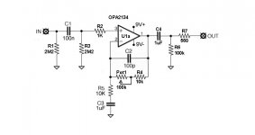
I've taken the liberty of redrawing your schematic. Interestingly, as you implement various changes this becomes more and more a bog standard preamp (buffer, whatever) circuit. This is not bad. Bog standard means "in accordance with the rules."
NOTICE that I've moved R2 to where I think it belongs. No other changes from your circuit. I think/hope the circuit notes might answer a lot of questions.
CIRCUIT NOTES:
R1 provides a load for the previous stage (in case one is needed), and together with R3 sets the input impedance (Zin). Zin is the parallel value of R1 and R3 (R1 || R3), in this case 1.1meg.
C1 blocks DC, and together with R3 forms a high pass filter, which in this case rolls off low frequencies starting about 10Hz. Guitars don't get within a mile of 10Hz, very few instruments do.
R3 provides a path for bias current, and together with R1 sets Zin as already noted.
R2: not sure. If it was 100 ohms I'd say it protects the op amp against drawing too much current, and helps prevent oscillation. I suspect that's what it's for anyway. Note that R2 started out on the upstream side of R3, but I've moved it to where I think it should be.
But...how can I think it should be someplace when I'm not sure what it's for? Well, I just do.
C2 shunts high frequencies around Pot1 and R4, increasing feedback for such frequencies, which decreases their amplitude at the output. This helps prevent oscillation, and can affect audio response if sized for that purpose.
U1 is the op amp, in this case an OPA2134.
Pot 1, R4, and R5 are the feedback network.
C3 blocks DC, and restricts DC gain to unity, which keeps DC errors from being amplified. It can affect audio response if sized for that purpose.
C4 blocks any DC that might be present at the output, especially including the DC errors that occur in all op amps. It can affect audio response if sized for that purpose...which in this case it is. Together with R6 it forms a high pass filter that, like C1-R3, rolls off around 10Hz. I don't know why.
R6: I have no idea what this is for, except to form a high pass filter. Some sort of tone shaping?
R7: not sure. If this was about 50-100 ohms I'd say it protects against the effects of capacitance on the output line. I suspect that's what it's for anyway.
.
Attachments
Last edited:
- Status
- Not open for further replies.
- Home
- Source & Line
- Analog Line Level
- Adding a (variable) gain boost to this non-inverting opamp buffer circuit?