Hi Mooly,
I'm glad you touched on HF oscillation. That could also cause higher current draw through the output stage.
The way that circuit is supposed to operate is that there will never be enough current in that leg to cause it to conduct. The event they are looking for is when the feedback loop is opened. Clipping does that, and the input stage will clip violently even if the outputs are just into clipping. This is the only time you would see all the tail current flowing through each of the diff poair alternatively. It's not supposed to be on a fine line between being triggered and ot. It doesn't have to be. Figure out the voltage drops at 1/2 the tail current. The diff pair normally doesn't swing around too much because of the giant amount of gain behind it. Again, the only time you have large current swings through the diff pair.
-Chris
I think the design falls down due to the deliberate unmatching of the diff pair which is crucial for low distortion. In this design the servo is forced to function in one quadrant.
Is it? or is it just being forced to operate offset because of something somewhere else in the amp. There are two feedback loops operating here. There is the main loop that couples the output back to the input differential amp, and then there is that silly integrator that further forces the output to be the same value as the input ground.
As I mentioned elsewhere, if the current sink Q108 is not sinking the design current, the output will try to go off center. The feedback will act to return the output to zero by unbalancing the input differential pair.
So maybe the amp was designed with the diff amp balanced - and if both sides of the diff amp were conducting the same amount of current, I don't think there would be an issue with the overload LED.
Last edited:
First, thank you all for sticking with me. It's clear that unlike many on this forum, I am not up to the level I should be for the diagnostics you are helping me with. Thanks, Mooly, for your explanation.
I haven't yet tried that; I pulled the KSC3503DSTUs from Q108/Q158 and measured those with my DCA75. The hFE was about 80, vBE 0.773, vCE 0.033, compared to hFE of 175 and 168, with lower vBE and vCE of the original 2SC2912 devices. I reinstalled those, and fired up the amp.
The leds take about 5 minutes and then glow so dimly I had to drape a blanket over me and the amp to see them.
I previously re-installed the original Q103/Q153.
I had originally changed D103/153 and D104/154 to 1N4148, based on discussions on this forum. I had also previously replaced D105/D155 with BA157, also based on this forum. The amp worked properly with those changes.
I will keep rolling back the active devices until I've gone back to all original. The diodes and e-caps have all been replaced.
No on the output transistors, but yes on the drivers. However, the amp worked perfectly with those drivers until the trace on the input board started this next phase.
...Armed with that information you could remove Q104 and measure the voltage across R106.
I haven't yet tried that; I pulled the KSC3503DSTUs from Q108/Q158 and measured those with my DCA75. The hFE was about 80, vBE 0.773, vCE 0.033, compared to hFE of 175 and 168, with lower vBE and vCE of the original 2SC2912 devices. I reinstalled those, and fired up the amp.
The leds take about 5 minutes and then glow so dimly I had to drape a blanket over me and the amp to see them.
...Q103 and D103/104 are critical and small differences away from the original design could well alter things enough to cause a problem.
I previously re-installed the original Q103/Q153.
I had originally changed D103/153 and D104/154 to 1N4148, based on discussions on this forum. I had also previously replaced D105/D155 with BA157, also based on this forum. The amp worked properly with those changes.
The first thing though is to see just how close to the trigger point it is running at.
I will keep rolling back the active devices until I've gone back to all original. The diodes and e-caps have all been replaced.
One more thing... hf oscillation could cause something like this to occur. Unlikely in itself but if you have changed any other parts (different output transistors and drivers etc) then its a possible.
No on the output transistors, but yes on the drivers. However, the amp worked perfectly with those drivers until the trace on the input board started this next phase.
The common thread seems to be that small changes in component operating parameters can cause the problem you're helping me with (the other common thread is I need to know more about SS topology and operation).
I began to think about the downstream component that I had changed that could affect the current draw - the indicator LEDs. When I got the amp, one of the originals had broken pins, so I replaced all LEDs. I have just swapped the good original for one channel, and after 30 minutes, it has not lit up at all, while the other has just the faintest glow I described earlier.
I have now measured the original and new LEDs and found the original had a vF of about 1.51v, but my replacements measure 2.01v.
Umm.
Hi Chris,
My point was that the original distortion LED is not lighting up at idle, but the new one is. Coincidentally, they have different vF, making me think the added current draw of the new LED is the cause of the remaining very faint glow, and perhaps the amp is not actually distorting?
Thank you,
Greg
My point was that the original distortion LED is not lighting up at idle, but the new one is. Coincidentally, they have different vF, making me think the added current draw of the new LED is the cause of the remaining very faint glow, and perhaps the amp is not actually distorting?
Thank you,
Greg
Last edited:
Hi Ylli,
The diff pair is where the input signal is compared to an attenuated version of the output. The only way this works properly is if the transistors in the diff pair are in fact matched and allowed to conduct equal currents. You can simulate this by assigning different values for beta in a normal design. Then try with matched transistors, then shift the operating current to one side or the other while watching distortion.
 Not 100% of course, but his book agrees with what I have seen in real life over decades. I think that on this point they are in agreement.
-Chris
Yes, in my opinion. The amplifier design is quite normal past the input stage. There is no technical reason to operate the amplifier with the diff pair purposely out of balance. If anything, this will increase distortion.Is it? or is it just being forced to operate offset because of something somewhere else in the amp.
The diff pair is where the input signal is compared to an attenuated version of the output. The only way this works properly is if the transistors in the diff pair are in fact matched and allowed to conduct equal currents. You can simulate this by assigning different values for beta in a normal design. Then try with matched transistors, then shift the operating current to one side or the other while watching distortion.
Yes, this is very common in amplifiers designed near the beginning of the 80's and newer. The main loop is supposed to control the audio signals. The offset part looks after the infrasonic frequencies. However, 99% of designs do not implement DC servos correctly. Look up the BGW 750C for an excellent example of how to do this correctly. They balance the amplifier so that the average output voltage from the op amp is low by adjusting the static predriver operating currents. Read the alignment instructions as the schematic is not clear on this. Once you understand this amplifier you'll know why most DC servo designs are basically wrong. After the previous experiments in the simulator you will understand how important keeping the diff pair balanced really is. An excellent book(s) are written by Doug Self. Read the one on amplifiers as it explains most of what you need to know. Bob Cordell also has an excellent book on power amplifiers. These two authors disagree strongly on a few things. I'm not going to say who I agree with <Self>.There are two feedback loops operating here. There is the main loop that couples the output back to the input differential amp, and then there is that silly integrator that further forces the output to be the same value as the input ground.
Not 100% of course, but his book agrees with what I have seen in real life over decades. I think that on this point they are in agreement.-Chris
Hi Greg,
The new LEDs might be throwing you off because they will light with less than 1 mA current. You might have a point there as that amount of leakage wouldn't affect an old style LED. Experiment with putting a resistor in parallel with the LED (on the PCB) to allow that minor leakage current to bypass the new LED.
-Chris
Hi Chris,
To clarify, put a resistor in parallel with R107 - 3.9k, or? Suggested value?
Thanks,
Greg
To clarify, put a resistor in parallel with R107 - 3.9k, or? Suggested value?
Thanks,
Greg
GKTAUDIO, please excuse the departure from the discussion at hand.
Anatech, thank you for your expanded explanation. I have 35 years in electronics, first 5 doing avionics repair and the next 30 doing RF/analog/a bit of digital work in an industrial environment (MRI systems). Mostly tech stuff, but some engineering and design work too. However, I have limited experience with consumer electronics and nothing really in the high end audio area. Some of the 'jargon' is unfamiliar to me, e.g. it took me a while to figure out what VAS was in regards to an amplifier.
I enjoy learning, and hope to be able to do that while participating in this (and other related) forums. I hope I am not creating problems by not necessarily approaching problems the same way that you more experienced guys do. But in the end, I am good at trouble shooting and find it fun to try and trace down issues.
In my job (retired 4 years now) I saw lots of circuits that were not as perfectly engineered as could have been, and tweaking part values to get things to play as desired was not uncommon and actually part of my job. But agree that doing that in a well designed circuit that has previously been working properly is probably not the best course.
Checked out the mentioned books. Would be nice, but the $$$ is a bit high right now.
Now back to our originally scheduled programing.
No worries, Ylli, I have so MUCH to learn, I am enjoying the wider discussion. Just wish I was more up to speed. You guys are fantastic for trying to help out.
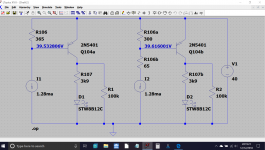
I just re-measured voltage across the resistors you suggested initially, and there are some slightly different readings from before.
R105 - 1.146
R106 - 0.454
R114 - 0.814
R155 - 1.136
R156 - 0.474
R164 - 0.818
I suppose I'll try Mooly's suggestion of pulling Q104 and measuring V across R106.
I just re-measured voltage across the resistors you suggested initially, and there are some slightly different readings from before.
R105 - 1.146
R106 - 0.454
R114 - 0.814
R155 - 1.136
R156 - 0.474
R164 - 0.818
I suppose I'll try Mooly's suggestion of pulling Q104 and measuring V across R106.
Last edited:
Hi Ylli,
No problem at all. Not knowing what your experience is, or anyone else reading these posts I try to explain most of what I'm trying to get at. So don't think I'm talking down to you. I'm just trying not to lose anyone.
Sorry about the jargon, occupational hazard as you well know.
As for modifications, something like an Adcom is well designed and there are thousands of these out there working fine as designed. Other brands need redesign from the ground up. Then there are those things I will change because we have better parts and techniques today than in the 70's (for example). However, I will never publish what I do because if something isn't working in a specific unit as expected, I can design my way out of it. Most people would just blindly follow instructions. Reasons why I would change something are
1.) clear performance increase with no detrimental effect on reliability
2.) to correct the cause of unreliable operation or short operating life
But, you can't assume you know better than the original design engineers, and you must be bloody certain that any changes will not adversely affect some functions or reliability. Making changes to a product is probably the one thing that can get you into trouble. I can't stress this enough. Never make changes lightly, and make sure you have the skill and instrumentation that backs up any tests you should make afterwards.
What I have written isn't directed at you Ylli, I'm trying to cover all readers of these posts.
-Chris
I believe your original numbers were something like:
R105 - 1.100 1.100/825 = 1.33 mA
R106 - 0.535 0.535/365 = 1.47 mA
R114 - 0.857 0.857/301 = 2.85 mA (1.33 + 1.47 = 2.80 mA)
R155 - 1.100 1.100/825 = 1.33 mA
R156 - 0.539 0.539/365 = 1.48 mA
R164 - 0.858 0.858/301 = 2.85 mA (1.33 + 1.48 = 2.81 mA)
New numbers:
R105 - 1.146 1.146/825 = 1.39 mA
R106 - 0.454 0.454/365 = 1.24 mA
R114 - 0.814 0.814/301 = 2.70 mA (1.39 + 1.24 = 2.63 mA)
R155 - 1.136 1.136/825 = 1.38 mA
R156 - 0.474 0.474/365 = 1.30 mA
R164 - 0.818 0.818/301 = 2.72 mA (1.38 + 1.30 = 2.68 mA)
Still unbalanced, but we've 'switched quadrants' - now there is more current in the input side compared to the feedback side. This change will work toward keeping the Distortion LED's off.
I just happen to have a GFA-555 II on the bench. I swapped in a few random LEDs from the parts bin, and some of them will glow faintly. In particular, a red high-efficiency was fairly bright.
I use Kingbright WP424HDT, Deep Red, and WP424YDT, Yellow.
I use Kingbright WP424HDT, Deep Red, and WP424YDT, Yellow.
A zillion posts since I last looked.
Who said 'new LED's'? That could definitely be a factor. As Anatech mentioned, new ones can be super efficient. I have some that are actually visible in the dark running from a 9 volt battery and with a series 10meg resistor.
Old LED's needed around 15 to 20 milliamps to illuminate 'brightly', a modern high efficiency one can do the same on just a few hundred microamps. Vf of the LED will make no difference here.
I see you measured 0.454v across R106. That's approaching the level a transistor will just about begin to turn on at... just about as in allowing a few microamps to begin to flow... and with a high efficiency LED its enough to get it to light.
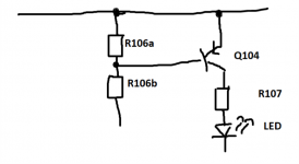
If you want to keep the bright LED's (and perhaps different transistors) then one fiddle would be to split R106 into two series resistors and add the B-E junction across the upper resistor.
Edit... (added) also look at the value of R107, the series LED resistor. 3k9 and the supply voltage (I don't know the value of that) determine the current but lets say it was +40 volts. That means a current of 10ma is available for the LED and that suggests a very low efficiency type common of that era. If the supply is higher than that then things are even worse with regard to modern high efficiency LED's
Who said 'new LED's'? That could definitely be a factor. As Anatech mentioned, new ones can be super efficient. I have some that are actually visible in the dark running from a 9 volt battery and with a series 10meg resistor.
Old LED's needed around 15 to 20 milliamps to illuminate 'brightly', a modern high efficiency one can do the same on just a few hundred microamps. Vf of the LED will make no difference here.
I see you measured 0.454v across R106. That's approaching the level a transistor will just about begin to turn on at... just about as in allowing a few microamps to begin to flow... and with a high efficiency LED its enough to get it to light.
If you want to keep the bright LED's (and perhaps different transistors) then one fiddle would be to split R106 into two series resistors and add the B-E junction across the upper resistor.
Edit... (added) also look at the value of R107, the series LED resistor. 3k9 and the supply voltage (I don't know the value of that) determine the current but lets say it was +40 volts. That means a current of 10ma is available for the LED and that suggests a very low efficiency type common of that era. If the supply is higher than that then things are even worse with regard to modern high efficiency LED's
Ylli,
Thank you very much for those calcs and your ongoing input!
Anatech,
Thank you as well for your continuing input and assistance. I know it's tough for you pros to dumb down things for the amateur.
Mooly,
Thank you very much for the drawing. I appreciate your time to sketch it out, and the pm for recommendations on resistance values.
Phloodpants,
Thank you for going to the trouble to swap out LEDs, and for the help you gave me earlier.
I'll report back as I move along.
Cheers
The split resistor reduces the Vbe available for the transistor like this. It doesn't look like much of a drop but it should be enough. If not, alter the ratios.
No disrespect, but how is this different than just changing R106 to 301 ohms as I suggested quite a bit back? The only difference is that just changing to 301 ohms would increase the collector voltage on the feedback side by 0.083 volts. The two collector voltages are already quite a bit different by design.
WHat you want to do is allow the leakage current around the new type LEDs. So a resistor in parallel will shunt the leakage down until the voltage across the LED is down to 1 volt or less. This will not hurt the actual operation indicating a peak.
-Chris
-Chris
- Status
- Not open for further replies.
- Home
- Amplifiers
- Solid State
- Adcom GFA 555 II - distortion indicators with no input signal