Unless you are using something like a current-feedback op-amp, every op-amp will also present that BW vs gain compromise, that is not unique to the AD8129. Also, a CMRR of 40dB at 100MHz is actually really good, parasitics really make it hard to maintain equal common-mode impedances at such frequencies, and, at those frequencies, the PCB and design also has a huge impact. Also, why do you care about 1/f if you are in the RF range? You might want to consider a hybrid discrete + opamp solution, that way you can lower the gain of the AD8129 and share it with a low-noise input transistor.
To be honest your specs don't make much sense to me, you mentioned previously you wanted audio range, and RF starting at 1 kHz? I don't understand, that is not even close to RF, and now you mention 100 MHz. I think there is some miscommunication going on.
To be honest your specs don't make much sense to me, you mentioned previously you wanted audio range, and RF starting at 1 kHz? I don't understand, that is not even close to RF, and now you mention 100 MHz. I think there is some miscommunication going on.
Look, I mentioned 3 different LNA's to build, as each with specific performances.
Now the current task is to build a LNA RF amplifier up to some xxx MHz or below 1 GHz.
The task is to measure the RF ripple on digital or analog LDO's.
Required is a differential AC input, (+) to go to Vpp and (-) to go to GND close as to (+) connections as with a 2.54 pin header.
Additional grounding shielding as freely connected as a differential probe from LeCroy AP034 but powered with gain (may 20..30dB).
Then, an op-amp is not the best solution for what you are asking.
You don't mention specific performances, you give figures like xxx MHz or below 1 GHz, that entails everything from 100-999 Mhz. Also, I gave you a recommendation on an op-amp with low 1/f noise, which is the first LNA you mentioned, yet, you said you are focused only on the RF LNA. Im am not sure what you want, but I think we are not going to reach an understanding.
You don't mention specific performances, you give figures like xxx MHz or below 1 GHz, that entails everything from 100-999 Mhz. Also, I gave you a recommendation on an op-amp with low 1/f noise, which is the first LNA you mentioned, yet, you said you are focused only on the RF LNA. Im am not sure what you want, but I think we are not going to reach an understanding.
Last edited:
The input voltage will be AC only. So to measure any RF ripple on 12V OXCO or on any ADC / DAC power.
I expect a maximal of 20...50mVpp ripple on those LDO's power output. The frequency base frequency of the MCK could be up to 100MHz as
some ADC/DAC clock needs.
For those high clocks as 100MHz, any 10 harmonics to measure. That's why 1GHz BW would be a nice to have.
This looks as a new field, as AKM & ESS & others do not specify the maximal ripple for those ADC /DAC chips.
Ok, things are making more sense now. What you want is not easy to do for several reasons:
- You mentioned 40 dB of gain, which is equal to a voltage gain of 100, that means you would need an op-amp with a Gain-Bandwidth product (GBW) of at least 100 GHz, AFAIK there is no such thing, but if someone knows of an op-amp with a GBW of 100 GHz, I would like to know. Even if you use two stages and split the gain, each with 20 dB, you would still need op-amps with a GBW of more than 10 GHz, since, in this case, the total attenuation at 1 GHz will be 6 dB not 3 dB. You might use more op-amps to increase the combined BW, but you would be also increasing noise, since the total Noise Figure deteriorates as you add more stages and the stages get reduced in gain. Op-amps are not high-frequency devices, so you are most likely going to have to resort to discrete components.
- Another problem is that 1 GHz is, in general, as high as you would like to go in an FR4 substrate, since the losses in the dielectric start becoming more relevant. Parasitics are also a big issue as frequency grows larger, which will deteriorate the CMRR and response of your circuit.
- If you want a proper amplifier with a relatively flat gain up to 1 GHz, you want to start thinking of transmission lines rather than PCB traces, this means that you need to be able to have a well-defined characteristic impedance for each line, and the specs of FR4 are not usually well-defined, plus, the permittivity of the dielectric in FR4 is most likely not constant or well-controlled. Typically, the permittivity in FR is around 4.5, but that is a ballpark figure, it could be considerably lower than that. If you need a high-end substrate for high frequencies you would have to buy a substrate from companies like Rogers, and they are most likely not going to sell it to you without a very good reason, so FR4 it is.
- There is the issue of impedance matching. At this point, I think it is not an exaggeration to state that what you are looking for is a low-noise microwave amplifier or at least very high RF (most people consider 1 GHz to be the dividing line between RF and microwave frequencies), so you may have to use RF techniques to design your amp, this means stuff like S-Parameters, impedance matching, Smith Chart, etc...
- At high frequencies amplifiers with negative feedback are harder to design, since we can no longer assume that a change of voltage/current in one part of a circuit causes an instantaneous voltage/current change in another part of the circuit. On top of everything there is the issue of stability, which is always a headache for RF designers.
So, to sum up, from what you have stated you want a high-frequency, low-noise, high and flat gain, differential RF amplifier with high CMRR and a 1 GHz BW. That is not easy to accomplish, not saying that it can't be done, but you can just go to Mouser or Digikey and buy an off the shelf part and drop it in a PCB willy-nilly. There are several considerations you should take into account. You may want to start looking for a high-frequency amplifier chip rather than an op-amp. AD sells some, but you can also look for products from high-frequency manufacturers like Mini-Circuits, they might have something that fits your needs.
Last edited:

Thank you!
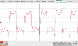
Here some measurements on my differential amp-probe (AD8129) and I need to consider your writings!
While I simple expected, that there are any new & better AD8129.
Also an issue IMHO, is the harmonic phase shift (s), as looking on the square signal as may distorted by the phase shifts f (freq).
Here some measurements on my differential amp-probe (AD8129) and I need to consider your writings!
While I simple expected, that there are any new & better AD8129.
Also an issue IMHO, is the harmonic phase shift (s), as looking on the square signal as may distorted by the phase shifts f (freq).
Attachments
After a year of frustration with the AD8428 design, I took a hint from @JensH's design as well as from Dick's website. The design isn't suitable for very low frequency measurements, which was the initial goal, but is more robust than the AD8428 and delivers repeatable measurements across the audio band. I'm thrilled. Thanks to everyone for sharing your expertise and pointing me in the right direction.

The below measurement was taken with the board in a Hammond 1455K1201 with neither end bolted on. The board is designed to slide right in, but I did not have the chance to mill the panels yet. So shielding is a far cry from the legendary cookie tin.

I attached the schematic with build notes and gerbers for anyone who may be interested in building one. Of course, feedback is more than welcome.
Some interesting learnings from initial prototyping:
The below measurement was taken with the board in a Hammond 1455K1201 with neither end bolted on. The board is designed to slide right in, but I did not have the chance to mill the panels yet. So shielding is a far cry from the legendary cookie tin.
I attached the schematic with build notes and gerbers for anyone who may be interested in building one. Of course, feedback is more than welcome.
Some interesting learnings from initial prototyping:
- I initially built it with an LT1806-- I had a bunch. It is an RRIO op amp and I suspect the open loop gain just isn't high enough. I only got 56dB of gain. Switching in an OPA132, which was also in the drawer, got me to 59.8dB. I'll say that's close enough. If I were to build another, I'd try an OPA1655 or similar, which has much higher open loop gain.
- I also used Kemet A750 al-poly input caps. Bad idea. The noise with the inputs shorted was about 3nV. I believe this is because of the caps' high leakage current. Switching in some plain old aluminum electrolytics brought tghe noise floor down to 300pV/sqrt(Hz).
- I'd like to try it with a couple of ZTX1051As. The boardband noise is higher, but the noise at 20Hz seems to be lower according to Dick's measurements.
Attachments
What PN of D1&2 ?.
The problem I see that there is no input protection. Simply connecting input to +5V and BJT 'd blow due unlimited base current.
Diodes help somehow if resistor 22 Ohm (from init post) returned, but still 1V jump at the base with emitter hardly tied to big C destroy B-E junction - guaranteed.
The problem I see that there is no input protection. Simply connecting input to +5V and BJT 'd blow due unlimited base current.
Diodes help somehow if resistor 22 Ohm (from init post) returned, but still 1V jump at the base with emitter hardly tied to big C destroy B-E junction - guaranteed.
Not sure what you are referring to with infinite base current. The schematic shows that the input is AC coupled. Do you mean the 5 V from the DC supply? that is fed via a 2 K resistor in series with a pot and another 10 K resistor and yet another 100 R resistor at the emitter, so even if one of the transistor B-E junctions shorts out, worst case scenario the current will be limited to roughly 300 uA.
" what you are referring to with infinite base current. The schematic shows that the input is AC coupled."
660 uF charging current at the moment of connection to DUT. 10V decoupled reference via ESR=100 mOhms or so provides 100 A impulse current spike.
660 uF charging current at the moment of connection to DUT. 10V decoupled reference via ESR=100 mOhms or so provides 100 A impulse current spike.
660 uF charging current at the moment of connection to DUT. 10V decoupled reference via ESR=100 mOhms or so provides 100 A impulse current spike.
Indeed, it's a tradeoff. Any series resistance on the input decreases the impulse current spike at the expense of increased noise. I'm using SB2H100 schottky diodes, which are rated for 75A peak forward surges because I happened to have exactly two. I didn't want to specify it on the schematic, because I'm sure there are better options. For what it's worth, I've tested multiple 9V power supplies and am pleased to report that the amp lives.
There's some more discusison on input protection starting at post #2.
Best practice would no doubt be to charge the cap through a resistor before taking measurements. A lower value input cap is no doubt fine, too, considering 1/f noise kicks in around 100Hz.
A 100 A spike to what? To the base of the transistors as you mentioned? No way. The example you gave is if you have a capacitor from input to ground with an ESR = 100 mOhms. That is not the case here. Because D1 and D2 are before the base of the transistors. Those diodes also have equivalent resistance, small, but they have resistance, so the current spike will be lower and they seem to be able to handle it, as the OP mentioned they have a 75 A rating. The voltage also gets clamped by the diodes to say 0.7-1.2 V. Again, far from unlimited base current, although I grant that it will stress the BJTs. So, yes, some extra voltage protection wouldn't hurt. Perhaps replacing the diodes with some Schottky's that can handle the current and produce a lower voltage drop?" what you are referring to with infinite base current. The schematic shows that the input is AC coupled."
660 uF charging current at the moment of connection to DUT. 10V decoupled reference via ESR=100 mOhms or so provides 100 A impulse current spike.
Last edited:
I see a lack of imagination here.
You don't understand that dynamic resistance of diodes makes situation worse, voltage pulse increasing over diodes. In next step this voltage pulse (over diode) via C7 680 uF generates base current - almost unlimited. In stationary condition C7 pre-charged, so 1-2 V over protection diodes summ up with 0.7V base-emitter to 1.7-2.7V. Now find low noise BJT that can handle 2V over B-E junction. If it's survive, it 'd not be low noise anymore."A 100 A spike to what? To the base of the transistors as you mentioned? No way. The example you gave is if you have a capacitor from input to ground with an ESR = 100 mOhms. That is not the case here. Because D1 and D2 are before the base of the transistors. Those diodes also have equivalent resistance, small, but they have resistance, so the current spike will be lower and they seem to be able to handle it, as the OP mentioned they have a 75 A rating. "
I'm thinking splitting 22 Ohm in two, than 1-2V over diode generates only 100-200 mA.Best practice would no doubt be to charge the cap through a resistor before taking measurements. A lower value input cap is no doubt fine, too, considering 1/f noise kicks in around 100Hz.
Attachments
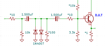
Aside from the insults on your side, I am having a hard time understanding what you are trying to say, as you do not write very clearly. I get it that extra protection is needed, as I have already mentioned it in my previous post, I granted that point. The schematic you posted does help ameliorate the problem, but it is useless. As this is supposed to be a very low noise amplifier. Having 20 ohms of series resistance at the input wreaks havoc on the noise figure. What good is to have a protected amplifier if it doesn't work for the application? The OP has already mentioned tests and the fact that he will be measuring voltage references not "Unlimited current" voltage supplies. How many voltage references do you know that can provide "Unlimited Current"?
Last edited:
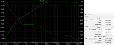

Thanks for sharing your sim! Here are some gain measurements using a 1mVRMS input signal.

.jpg")
I think you may have shifted a decimal on C11 in your sim; it's a dozen 2.2mF caps, which works out to 26.4mF rather than 2.64mF. This capacitor is what limits the low frequency response of the LNA, as it increases the amount of feedback as its reactance approaches 1 ohm (R8).
My measured f3 is around 8Hz. Increasing C11 should result in a lower f3, which is why I'd encourage anyone considering building one to look into those 4700u caps which fit the same footprint. I'm not sure if the ZTX851 has a low enough 1/f noise for it to be worth pursuing.
Also note that, while it probably won't matter for yourt sim, the op amp runs right off of the 9V battery rather than off of the regulated 5 V supply. You may also wish to increase the value of R2 to center the output of the op amp around 1/2 of its supply voltage.
What is the advantage of using the 12 x 2200uF capacitors in parallel with 100 ohm compared to using a servo as I did?
What is the advantage of using the 12 x 2200uF capacitors in parallel with 100 ohm compared to using a servo as I did?
I didn't mean to imply that it was an improvement over your design when I referenced it earlier; my apologies if it came off that way.
For the same transistor running the same current, your design wth the servo had a higher 1/f corner than the measurements published for the ZTX851 in AoE and on Dick's website. In my mind, this meant that there was something about the biasing scheme that was increasing noise above the transisfor's voltage noise.
I ended up building your design on a breadboard and tried to tweak values to improve the low frequency noise, but had some trouble getting it to bias after making changes. My sense was that fewer feedback loops meant that fewer things could go wrong, and so I opted for lots of capacitance and a single op amp (rather than compound) instead. It's inelegant, but a bit easier for me to wrap my head around.
- Home
- Design & Build
- Equipment & Tools
- AD8428 Low Noise Preamplifier