Re: How do I calculate the compensation capacitor?
Hi Oli,
As I said the compensation cap can be part of the analog low-pass filter. Just fill in the appropiate crossoverfrequency and type and order of filter in FilterPro.
The minimal value for Ccomp is 100-330pFwith a 3k feedback resistor.😎 😎 😎
Oli said:I I would like to calculate a suitable compensation capacitor. The data sheet gives confusing information about the choice of compensation capacitor (The formua makes no sense). Is there a formula for choosing an appropriate capacitor at Iout and a compensation capacitor for a given opamp and desired transfer function.
Hi Oli,
As I said the compensation cap can be part of the analog low-pass filter. Just fill in the appropiate crossoverfrequency and type and order of filter in FilterPro.
The minimal value for Ccomp is 100-330pFwith a 3k feedback resistor.😎 😎 😎
Could 2nd order MFB provide a solution?
Elso,
After dabbling with the idea of discrete I-V conversion I have decided to keep things simple and stick to op-amps
I have just been playing with Filterpro and instead of first order circuit I have been experimenting with 2nd order MFB. This arrangement rather neatly shunts RF to ground via a capacitor before the feedback loop (hence reducing TID). The capacitor in the feedback loop provides a the second pole of the filter and appropriate phase compensation.
My only question is - Is such a second order filter, with input resistors a virtual ground for the current output of the AD1865k?
I am getting there slowly!
See AD797 datasheet
Analogue Devices use the technique mentioned in my previous question in the AD797 data sheet (Audio DAC application).
Does this provide a clue for the formulas I need to get a Bessel filter with a desired -3dB cutoff for this 2nd order filter?
Nobody yet seems to know the answer- perhaps the output impedance of the DAC itself forms part of the filter?
Re: Could 2nd order MFB provide a solution?
No. There will be a varying, frequency dependant impedance.
Best solution is to use a) No analog filter 1 x opa
b) 1st order (c parallel to FB R) 1 x opa c) 3rd order,
2 x opa, 1st opa has single pole as in b) and second opa follows
with additional 2 orders.
If you are running tube stuff, often no filter is fine!
Cheers,
Terry
Oli said:Elso,
After dabbling with the idea of discrete I-V conversion I have decided to keep things simple and stick to op-amps
I have just been playing with Filterpro and instead of first order circuit I have been experimenting with 2nd order MFB. This arrangement rather neatly shunts RF to ground via a capacitor before the feedback loop (hence reducing TID). The capacitor in the feedback loop provides a the second pole of the filter and appropriate phase compensation.
My only question is - Is such a second order filter, with input resistors a virtual ground for the current output of the AD1865k?
I am getting there slowly!
No. There will be a varying, frequency dependant impedance.
Best solution is to use a) No analog filter 1 x opa
b) 1st order (c parallel to FB R) 1 x opa c) 3rd order,
2 x opa, 1st opa has single pole as in b) and second opa follows
with additional 2 orders.
If you are running tube stuff, often no filter is fine!
Cheers,
Terry
Thanks Terry!
Thanks Terrry. I am using transistor amplification and will probably go for a first order filter with C parallel to Rfb around the OPA. This currently works on my prototype with no obvious distortion. I just felt a little more could be achieved by shunting RF straight to ground before the OPA. Out of interest, do have a look at the aforementioned Analogue Devices application note. Clearly the maths exist somewhere to perform the required 2nd order filter with no resistors at the input of the OPA- hence a virtual ground exists. This novel circuit includes the RF reducing capacitor.
Thanks Terrry. I am using transistor amplification and will probably go for a first order filter with C parallel to Rfb around the OPA. This currently works on my prototype with no obvious distortion. I just felt a little more could be achieved by shunting RF straight to ground before the OPA. Out of interest, do have a look at the aforementioned Analogue Devices application note. Clearly the maths exist somewhere to perform the required 2nd order filter with no resistors at the input of the OPA- hence a virtual ground exists. This novel circuit includes the RF reducing capacitor.
A possible solution relating to my previous quesions on this thread....
'The use of a capacitor across I-V conversion op-amp input to shunt noise directly to ground and produce a 2nd order response'
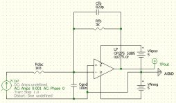
I have been busy this week, but I spent some time studying the maths relating to my problem. Eventually, however, I thought of solving the problem empirically using spice simulation. I used WinSpice shareware and downloaded spice models of real op-amps from various manufacturers. The individual behaviour of the op-amp is critical to the choice of component values. In the attached picture I have chosen an OP275 for example purposes only- I will possible use AD8610. The 1.8K resistor is the Thevenin equivalent of the output impedance of my AD1865 DAC.
'The use of a capacitor across I-V conversion op-amp input to shunt noise directly to ground and produce a 2nd order response'
I have been busy this week, but I spent some time studying the maths relating to my problem. Eventually, however, I thought of solving the problem empirically using spice simulation. I used WinSpice shareware and downloaded spice models of real op-amps from various manufacturers. The individual behaviour of the op-amp is critical to the choice of component values. In the attached picture I have chosen an OP275 for example purposes only- I will possible use AD8610. The 1.8K resistor is the Thevenin equivalent of the output impedance of my AD1865 DAC.
Attachments
There's more....
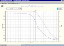
Here is the resulting response curve (See attached picture)
What does everyone think of this method?
I am striving for a transient perfect response. What does this look like on such a graph?
(I think... the phase characteristic around the -3dB cutoff frequency will have perfect symmetry like in my example - True or false?)
Attachments
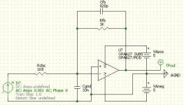
Check out the reponse curve..
The -3dB cutoff is rather high, but I wish to reduce phase shift at 20kHz.
Note how the phase response looks flatter and overall more linear. This linearity, however is not centred at the -3dB frequency. In addition, phase shift at the -3dB frequency is not 90 degrees.
Which of my plots represents a better transient response?
Attachments
Built it!
I have just finished building and listening to the later circuit. It certainly sounds better than the internal I-V conversion- more highs, greater depth, transparency and deeper bass. The slight grittiness that existed before has gone!
A word of caution- Initially the DC offset was a large 27mV. This was remedied using DC offset correction as suggested on the Burr Brown datasheet.
The characteristics of the OPA627 are apparent- Almost too hi-fi. The bass is a little overblown. I can live with this sound and it is certainly a better overall choice than the internal converter. I think I will try the AD1865, however, as I have read claims of a more natural sound.
BTW does anyone have the answer to my aforemention question:
What does the phase response look like for a perfect transient response?
Grounding confusion
It has been a while since I wrote in this forum.
It is interesting to read some of my previous correspondance and my misconceptions at the time!
Progress with my AD1865 DAC has been slow but steady.
I am still using OPA627s as I/V conversion- Nothing else seems so transparent.
I wish to do the 'proper thing' when decoupling the supplies of the OPA627s. Currently I am connecting a ceramic capacitor directly between +v and -v. I believe Kui Yung Wang uses this arrangement.
Would it be better to connect a capacitor between +v and ground and another capacitor between -v and ground?
If so, should I decouple using the Right and Left ground pins of the AD1865 (for better separation), rather than the central analogue ground point? If I do use the Right and Left ground pins to decouple noise from the supply lines am I in danger of polluting my I/V converter. The non-inverting input of each opamp is tied to these Right and Left ground pins of the AD1865.
Any thoughts- I am quite confused
😕 😕
Hi Oli,
I am also currently using opa627 as I/V for my AD1864 within my Proceed DAP and alsoare looking intothe best way to decouple them. The Proceed uses a decouple cap between +12 and -12V. I replaced this by two caps between +12 and grnd and -12 and grnd. Because I want to change the grounding within the DAC I run into an article of Analog Devices,which has some interesting comments on both the grounding and decoupling. (I don't have the link here, but the name of the articleis: "An IC Amplifier User's Guide to Decoupling, Grounding and Making Things go Right for aChange'. AsI understand the article correctly it tells that you should decouple the V- in case of opamps that use PNP-transistors as input (negative supllycoupling) and V+ in case of NPN-transistors. (positive supply coupling). The cap should in both situations be as close to the V+ or V- railas possible.
Hope the article provides you some more hints.
Some good grounding ideas!
Calimero,
Thanks for the info. I have just read the data sheet from the Analogue Devices website. Indeed this does suggest decoupling -ve to ground for the PNP topology. It also shows a capacitor connected directly between +ve and -ve and not between +ve and ground. This seems strange- I wonder why Burr Brown, Analogue Devices and other manufacturers suggest +ve to ground in so many of their application notes when a direct +ve to -ve connection appears to be superior?

Note the method of separating power ground and signal ground. This should avoid polluting of my opamp's non-inverting input. Just to add to my confusion a special method is suggested for virtual ground type circuits. I am presenting my DAC with a virtual ground using the OPA627 as an I-V converter.

Calimero,
Thanks for the info. I have just read the data sheet from the Analogue Devices website. Indeed this does suggest decoupling -ve to ground for the PNP topology. It also shows a capacitor connected directly between +ve and -ve and not between +ve and ground. This seems strange- I wonder why Burr Brown, Analogue Devices and other manufacturers suggest +ve to ground in so many of their application notes when a direct +ve to -ve connection appears to be superior?
Note the method of separating power ground and signal ground. This should avoid polluting of my opamp's non-inverting input. Just to add to my confusion a special method is suggested for virtual ground type circuits. I am presenting my DAC with a virtual ground using the OPA627 as an I-V converter.
Mistake on AD1865 data sheet?
I'm ready to order parts for the AD1865N-K DAC project.
Suddenly I've had a moment of doubt....
The data sheet states a minimum 13.5Mhz operating frequency.
😕 Is this a mistake?😕
😕 do they really mean maximum frequency?😕
I'm ready to order parts for the AD1865N-K DAC project.
Suddenly I've had a moment of doubt....
The data sheet states a minimum 13.5Mhz operating frequency.
😕 Is this a mistake?😕
😕 do they really mean maximum frequency?😕
No longer confused
😀 😀 😀
No longer confused!
The guys at Analogue Devices have clarified the matter.
13.5Mhz refers the mimimum specified operating frequency.
i.e. the DAC will handle frequencies up to this minimum limit.
A rather poor way of describing this parameter if you ask me

😀 😀 😀
No longer confused!
The guys at Analogue Devices have clarified the matter.
13.5Mhz refers the mimimum specified operating frequency.
i.e. the DAC will handle frequencies up to this minimum limit.
A rather poor way of describing this parameter if you ask me
- Status
- Not open for further replies.
- Home
- Source & Line
- Digital Source
- AD1865N-K dac Project