A lock washer between the RA terminal and the binding post should hold it securely once tightened,
without any soldering. Or install a washer and KEP nut on the other side, tightened with a nut driver.
without any soldering. Or install a washer and KEP nut on the other side, tightened with a nut driver.
Last edited:

Super interesting thread! I had been considering building two ACA monoblocks (1 board per) and I love the form factor. It looks like the standard ACA board will fit nicely on the larger heatsink they sell--and allow some upgrades (a-la-ACA/w premium parts). Having built a couple of kits, fabbing a round chassis for this heatsink would be a fun project--I'm not scared of wiring the inputs/outputs. My question is: is this circuit the same circuit as the regular ACA board, or has it been modified? I'd love to hear two of these powering my open baffle speakers. Thanks for the creativity! JS
My question is: is this circuit the same circuit as the regular ACA board, or has it been modified?
It's the same circuit as the pcb you can find in the store, ACA 1.6
My first revision in the first post has lower output capacitance, but that will change back to the standard 3300uF in the next revision.
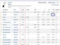
It might be fun to revise the circuit, to take advantage of now-available-again, very low cost J111 N-channel JFETs in thru hole packages. They are substantially cheaper than Toshiba 2SK170 and Linear Systems LSK170. J111s work very well as source followers, which is exactly how the 2SK170 is used in the ACA. And since the ACA circuit already includes an adjustable resistor (trimmer) to deal with manufacturing variability of this JFET, it's practically a drop-in, plus adjustment of ancillary resistor values.
At USD 14.00 per hundred transistors, they're a bargain. So compelling in fact, that I've purchased 500 for my own experiments and future projects. And the Pchannel J175 is now available again too -- I've bought bunches of them as well. Just in case of continuing spotty supply.
Mess around on octopart dot com and/or findchips dot com, you'll see loads of thru hole, non Toshiba JFETs at wonderful prices. Example below.
_
Attachments
I selected a heatsink meant for LED lights. Typical "grow light" heatsinks are now produced in large quantities and are one of the more economical large passive heatsinks available. The one I've selected is a circular forged pin heatsink 120mm diameter and 70mm tall (4.7" × 2.75"). I estimate its thermal resistance at around 0.9°C/Watt. It cost $19 with free shipping.
Hi Mr. Brock, I wonder whether this is the heatsink you are talking about?
https://www.aliexpress.com/item/32947619807.html
_
Attachments

Hello Mark,It might be fun to revise the circuit, to take advantage of now-available-again, very low cost J111 N-channel JFETs in thru hole packages. They are substantially cheaper than Toshiba 2SK170 and Linear Systems LSK170. J111s work very well as source followers, which is exactly how the 2SK170 is used in the ACA. And since the ACA circuit already includes an adjustable resistor (trimmer) to deal with manufacturing variability of this JFET, it's practically a drop-in, plus adjustment of ancillary resistor values.
What has to be done after replacing the 2sk170 by the j111 - excepted adjusting the trimmer ?
Thanks !
While I can (usually) build the NP amps we all discuss here, I continue to be in awe of the creativity I see here.
Well done, and way to think “outside of the box”!
Well done, and way to think “outside of the box”!
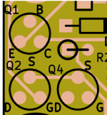
IIRC the J111 has the Gate on one side while the 2SK170 has the Gate in the middle. So installing the J111, you end up with crossed legs. A pet peeve of mine, you wouldn't have this problem if you used a triangular pattern for the leads on the PCB. You can just rotate the part. Move the middle hole/pad 0.1 inch to the flat side of the TO-92. As a bonus, you can use bigger pads on the PCB. That makes soldering easier and less damage to the PCB if you have to remove the part. You can even make the layout compatible with SOT-23's mounted on the solder side.
Yep, that idea was used on the M2x daughter card named IPS6, whose PCB layout Gerbers were posted to diyAudio in August 2020 . Circular footprints which accept all permutations of pin ordering, were used for both JFETs (Q2 + Q4) and also BJTs (Q1). Since 2N transistors have a different pin ordering than European BC transistors, which are both different than the pin ordering of Japanese 2SC and 2SA transistors.
_
_
Attachments
- Home
- Amplifiers
- Pass Labs
- ACA Redux