
In theory, if the bridge is balanced, there should be no current required for the voltage amp. Yet, in #13 we see over 100 ma RMS current from the voltage amp. What is going on? Here is little insight about this.
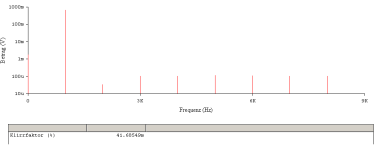
If you probe the bridge, you will see there is a voltage ripple with 90 degree phase shift. The orange trace below is from the bridge. The red trace is at the output.

The amplitude of the "imbalance" is 13mv above. That means there has to be some current from the Voltage amp (N2) to sink 13mv peak offset. Thus, the current is 13mVp / (R1 // R2). From my post #13, R1 is 0.1 Ohm, R2 is 0.33 Ohm. It is about 168ma peak, which is about the same value we see from the simulation.
(I borrow the bridge diagram from #20)

The imbalance signal peaks at the crossover region where it needs the most slew rate. Fortunately, it just happens to be a formula between the slew rate and the differential input voltage.
By given an amp with input stage that has transconductance (gm) followed by miller compensated (Cdom) VAS, the slew rate = (Vin_pos - Vin_neg) * gm / Cdom, where (Vin_pos - Vin_neg) is the imbalanced voltage.
Also, the peak slew rate of the output sine wave is 2 * pi * f * A, (where the A is the amplitude).
Combining the 2 conditions above, you get:
Vin_pos - Vin_neg = (2 * pi * f * A) * Cdom / gm
Note that 1 / (2 * pi * Cdom / gm ) is also the bandwidth (BW in Hz) of the amp (N1).
Thus
Vin_pos - Vin_neg = A * f / (BW)
Let's say BW is 10MHz (in the case of NE5532), f = 10KHz, A = 10 Vp. The offset would be 10mVp based on the formula above. I call it is close enough to the simulation.
The max of A (amplitude) is defined by the power rating of the entire amp. The max of f is 20KHz, in general.
If you want to minimize the offset, the only thing you can control is the bandwidth of the current amp (N1).
So far, the bridge is a bridge made of resistors only. Maybe there are some advanced bridges that with cap and coil, we haven't investigated yet.
If you probe the bridge, you will see there is a voltage ripple with 90 degree phase shift. The orange trace below is from the bridge. The red trace is at the output.
The amplitude of the "imbalance" is 13mv above. That means there has to be some current from the Voltage amp (N2) to sink 13mv peak offset. Thus, the current is 13mVp / (R1 // R2). From my post #13, R1 is 0.1 Ohm, R2 is 0.33 Ohm. It is about 168ma peak, which is about the same value we see from the simulation.
(I borrow the bridge diagram from #20)
The imbalance signal peaks at the crossover region where it needs the most slew rate. Fortunately, it just happens to be a formula between the slew rate and the differential input voltage.
By given an amp with input stage that has transconductance (gm) followed by miller compensated (Cdom) VAS, the slew rate = (Vin_pos - Vin_neg) * gm / Cdom, where (Vin_pos - Vin_neg) is the imbalanced voltage.
Also, the peak slew rate of the output sine wave is 2 * pi * f * A, (where the A is the amplitude).
Combining the 2 conditions above, you get:
Vin_pos - Vin_neg = (2 * pi * f * A) * Cdom / gm
Note that 1 / (2 * pi * Cdom / gm ) is also the bandwidth (BW in Hz) of the amp (N1).
Thus
Vin_pos - Vin_neg = A * f / (BW)
Let's say BW is 10MHz (in the case of NE5532), f = 10KHz, A = 10 Vp. The offset would be 10mVp based on the formula above. I call it is close enough to the simulation.
The max of A (amplitude) is defined by the power rating of the entire amp. The max of f is 20KHz, in general.
If you want to minimize the offset, the only thing you can control is the bandwidth of the current amp (N1).
So far, the bridge is a bridge made of resistors only. Maybe there are some advanced bridges that with cap and coil, we haven't investigated yet.
Last edited:
quick answer:Maybe there are some advanced bridges that with cap and coil, we haven't investigated yet.
there are ones! Very similar to the dumper - and that's not really surprising.
quick answer:the only thing you can control is the bandwidth of the current amp (N1).
This is exactly how it is handled in practice (the Technics amplifier class aa series).
Be careful, I'm totally out of practice
The following should apply:
R2 smaller than Zload
and
(R3/R4) less than or equal to (R1/R2)
with
k = (R3/R1) * (R2/R4)
but the following also applies
k = |(R2/Zload)|
from this follows the paradox Zload = R1*R4 / R3 !
But our goal should be that |Iout(N2)| tends to zero.
R1 may be expressed as Z1, and R3 as Z3; to put it simply: C in parallel with R3 and L in series with R1.
Now it gets tricky and jOmega or S comes into play.
I think Marcel ( @MarcelvdG ) is fully in the exercise - he could help us with the most optimal balancing and dimensioning condition.
We are looking for Z1, Z2, Z3, Z4 all from S or jOmega, ..!
Last edited:
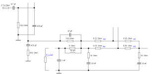
With R1=0.5Ohm, R2=1/2 * R1 and R3=10 * R1, R4 =1/2 * R3 we can easily calculate statically how the combination of N2 and N1 will behave.
In this case, RL is transformed by a factor of 10.25, in other words: N2 must be able to draw 1/10 of the required load current!
In any case, this is sufficient to bias the B output stage (N1 indirectly, on the output side) in such a way that N1 generates practically no transfer distortion.
In the case of zero, i.e. the zero crossing, you can simply throw away N1 (practically with R1, R3, R4), then R2 and ZL=RLoad remain, now a constant current flows through R2, namely Vout/ZL, with Vin = Vout. The familiar rules for voltage dividers apply. ZL determines the current!
In this static case and moment, N2 works as a class A representative all by itself on the load, the Iq of greater than 70mAdc is now completely sufficient to carry out zero crossing without complaint under all circumstances.
However, due to the miracle of the magical feedback and the enormous DC gain (I hope this is the correct way to say it) of N2 (& N1), N1 will not be able to stay out of the matter at all.
In the ideal scenario /the imagination above, the amplification (the Bridge) is always well balanced (controlled). So no transfer distortion ---> just perfect A operation.
#
However, this does not mean that the final transistors of the control amplifier N2 do not require a sufficiently dimensioned heat sink, on the contrary - you should expect maximum losses of 15Wrms at full scale if equalizing currents are flowing!
Attachments

Simulation results below - each with an LF356 vintage OP amp and RLoad = 8Ohm.
Addendum to posting #26, it is best to consider three starting points
a) with R1 = infinity in the static analysis and calculate
a.1) R1 to 0.555Ohm
b) with R1
c) and now with ri_N1= infinity ..!
Addendum to posting #26, it is best to consider three starting points
a) with R1 = infinity in the static analysis and calculate
a.1) R1 to 0.555Ohm
b) with R1
c) and now with ri_N1= infinity ..!
Attachments

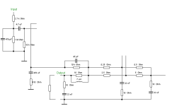
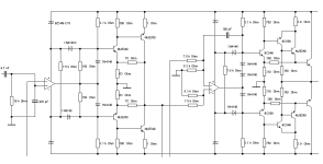
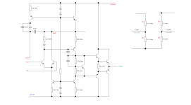
Proof of concept
At first glance, you recognize two rather questionable amplifiers, each an antiquated op-amp with an adventurous afterburner. Both amplifiers are, each on its own, deliberately oddly designed. Neither would be a commendable design on its own and without the bridge. And that is exactly what was intended. Errors (i.e. distortions, instabilities ...) are supposed to be retouched and virtually regulated away by feedforward and gnfb.
The tip to oscilloscope and analyze the bridge voltage is spot on, the bridge is the be-all and end-all.
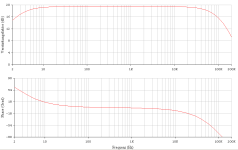
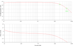
As expected, the bandwidth is severely limited, but sufficient. Who wants to unleash fsignal= 20kHz on the tweeter with 50 watts? So I deliberately set the bandwidth to fo 50kHz. Here the bridge signal is already 100mVac, in the sensitive audio range it is 1mVac.
tbc
At first glance, you recognize two rather questionable amplifiers, each an antiquated op-amp with an adventurous afterburner. Both amplifiers are, each on its own, deliberately oddly designed. Neither would be a commendable design on its own and without the bridge. And that is exactly what was intended. Errors (i.e. distortions, instabilities ...) are supposed to be retouched and virtually regulated away by feedforward and gnfb.
The tip to oscilloscope and analyze the bridge voltage is spot on, the bridge is the be-all and end-all.
As expected, the bandwidth is severely limited, but sufficient. Who wants to unleash fsignal= 20kHz on the tweeter with 50 watts? So I deliberately set the bandwidth to fo 50kHz. Here the bridge signal is already 100mVac, in the sensitive audio range it is 1mVac.
tbc
Attachments
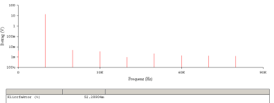
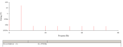
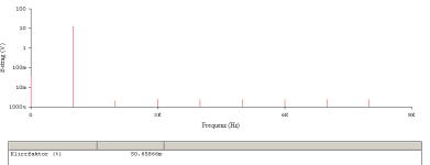
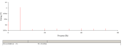
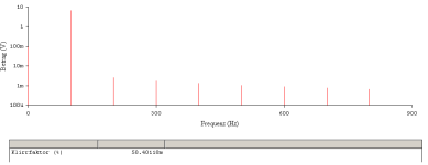
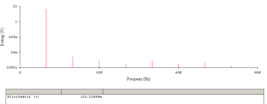
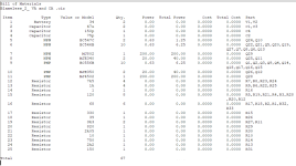
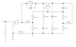
A few results, FFT using old spice - they should give nothing more than clues.
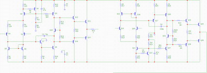
The so-called current amp is made up of an LF356 with an additional voltage-amplifying push-pull output stage. Voltage dividers at the inputs should ensure that the maximum input voltage range of the integrated op-amp is not exceeded. The supply voltage fluctuates, but does not exceed +/-18Vdc. However, the Z diodes must be able to convert losses of up to 1W. The OLG is approximately 112dB. Iq of the strange output stage is less than 30mAdc.
The so-called voltage amp follows the same scheme, it lacks an EF on the output side - it doesn't have to do anything. OLG also 112dB, Iq greater than 70mAdc. Let's just say it's class A.
tpc
Attachments
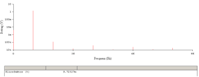
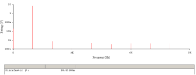
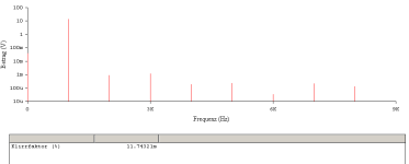
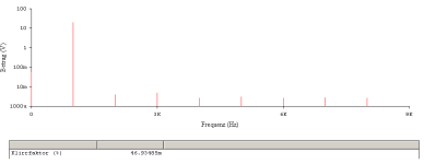
The FFT (a simulation) can certainly be improved by optimized, tricky parameter settings - lower THD!
But we are only talking about reference points. And the bottom line is: Class AA (just an advertising name, just like all the others, for example Current dumping or Class AB-BA double cross) works fantastically well - it catapults even this catastrophe to more than usable heights. With sub-amplifiers optimized and dimensioned for the purpose (i.e. N2 - Voltage Amp & N1 - Current Amp), a heavenly THD of 2m%, -94dB under full scale /load and bandwidth can be easily achieved via a perfectly balanced bridge (our feedforward), this was the standard specification in the 1980s for this type of Japanese amplifier.
Perhaps it is worth thinking about this forgotten path again.
Finally, seemingly bad values, seemingly ...
Bye,
HBt.
Attachments
Do you bootstrap the opamp just like SE-A100?
That bootstrap scheme only works for the original opamp model. It tends to oscillate with others.
That bootstrap scheme only works for the original opamp model. It tends to oscillate with others.
I don't think we'll need a bootstrap (nor a dynamic level shifter, I think that's what you're trying to say with the bootstrap: “the rails follow the level /modulation /swing of the signal”).Do you bootstrap the opamp just like SE-A100?
That bootstrap scheme only works for the original opamp model. It tends to oscillate with others.
Nothing is allowed to vibrate/ swinging / or oscillate here - no dynamic instabilities, I spent half the night observing the bridge-voltage ... the dimensioning of the bridge is still giving me a headache, probably because it seems to be trivial. But everything has to fit here.
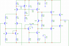
Let's start with a little blameless VA.
@jxdking
please also look in the service manual of the amplifier SU-V40,50,60 and SU-VX800, especially the latter.
regards,
HBt.
PS
Can we already issue guidelines?
Attachments
Last edited:
I can live with VA, CA all virtual opamps for now and don’t worry about voltage rating. They can be implemented with discrete circuitry later on and should not be a problem to study class AA.Let's start with a little blameless VA.
Before diving into the bridge with caps and coils, just with the resistant bridge, the current supplied by VA is too much as I like.Can we already issue guidelines?
The blameless recipe and the well-known topology
One can't go wrong with this dish, it always works:
hardly any more components than in the "3/4 + 3/4 Ampflifier project", I create a new workingbase in advance, 3/3 + 3/3 equal a whole of 1VA + 1CA ..!
One can't go wrong with this dish, it always works:
hardly any more components than in the "3/4 + 3/4 Ampflifier project", I create a new workingbase in advance, 3/3 + 3/3 equal a whole of 1VA + 1CA ..!
Attachments
I think so too, the output current to be supplied by the VA (N2) should tend towards zero. That would be the theoretical ideal, but it is practically impossible. At the same time, we must avoid creating virtual negative internal resistances.Before diving into the bridge with caps and coils, just with the resistant bridge, the current supplied by VA is too much as I like.
HBt.
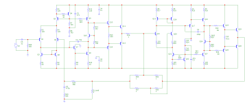
The INTEGRATED
The SVI also contains the bridge, but not the very simple +Vcc'bootstrap of the IP-VA stage already shown below - this is realized externally.
FYI
- use the IC AN7062N (Panasonic) directly followed by an external EF2 - this is the class A voltage amp (N2)
- and the smd-equipped SVI4004 (Sanyo?) hybrid circuit (labeled with the "Class AA Current Drive" seal) - this is the Class B current amp (N1)
The SVI also contains the bridge, but not the very simple +Vcc'bootstrap of the IP-VA stage already shown below - this is realized externally.
FYI
Attachments
- Home
- Amplifiers
- Solid State
- AA50W - A conceptual idea