I'm putting together a drive card intended to drive a couple of sets of TO-3 lateral fets for about 100W/channel. I have some nice heat sinks that take two TO-3 packages apiece, so four of them would work for a stereo amplifier.
I may make some changes in the architecture and stuffing (mosfets for diff pairs instead of bipolar?). Instead of using a single master current source to bas the differential pairs, I may use a couple of ring-of-two sources (slightly more simple). I'll be filling in more values as I continue.
I may make some changes in the architecture and stuffing (mosfets for diff pairs instead of bipolar?). Instead of using a single master current source to bas the differential pairs, I may use a couple of ring-of-two sources (slightly more simple). I'll be filling in more values as I continue.
Attachments
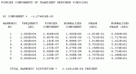
I went ahead and ran a sim on the circuit shown earlier using dummy parts form the PSpice library and power Darlington outputs. The purpose was to see if the input diff stage balanced, and to adjust values for appropriate bias levels. I found that an alternate connection for the diff pair cascode bias resulted in lower distortion. I'll post the results when I get home.
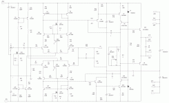
OK - here's the PSpice sim I ran to establish balance and bias levels for the finished amp. The sim works well with standard power Darlington outputs. This might be an option for another amp entirely... Here, though, the objecitive is to set bias levels for an input/drive card for a lateral FET amp of ~100W/channel.
Attachments
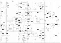
I updated the layout to either work with Zetex/Diodes, Inc. small-signal mosfets, or MPSA15 and MPSA64 Darlingtons. This change helps to reduce the capacitor size in the feedback network. I also pused the input transistors closer together and turned them around so that I can use thermally coupled matched pairs. Layout is actually done, and I'll give it another once-over and perhaps order PCBS this weekend.
Hi, Wrenchone,
I have a few comments on this design. It has good bones, but a few oddities in the details.
I'm glad you changed the biasing scheme for the input pair cascoding. The one in your first schematic was not going to work. 7V Zeners should work OK. The NPN input cascode would have worked with a couple of diodes in series with the emitter of Q23.
The PNP input cascode needed an NPN in place of the "other" Q23, wired like the other one, and with a couple of diodes in series with the emitter.
In your latest posted schematic, resistors R17, R18, R28, and R29 should be removed and shorted. They don't really do much of anything, but what they do is undesirable.
The zeners should work OK to bias the input cascodes, but I like the original idea better of having their bases float with the common-mode input voltage.
The buffered cascoded VAS looks nice, except that the 7V zeners biasing the cascodes are really going to limit your output signal swing. I would use 3 regular diodes or maybe a GREEN LED. in place of D1 and D2. Nothing larger than 2.5V or less than 2V. Again, short the resistors R40 and R47. They do almost nothing, and what they do is not wanted.
Be sure to calculate the power dissipation of transistors and resistors, size, and sink appropriately. You probably know that Q21 and Q24 dissipate about 0.4W, and Q22/Q23 dissipate about 1.2W each. R52 dissipates about 1/2 W. A little more if you replace D1 and D2 with something a bit lower voltage.
Finally, I'm curious about your use of Darlingtons for the output transistors. Output triples are tricky enough without Darlingtons. Have you checked the stability of this output triple? It might be fine because the driver transistor (within the Darlington) in the triple is quite band-limited, compared to the final and the pre-driver. Be prepared to to put a Zoebel around those Darlingtons, either from base to emitter or from base to collector. Also be prepared to give up on Darlingtons and replace them with simple transistors, if you cannot get them to work right.
I ran across the PCBs I designed for this project last night, and had to do a deal of searching through my archives before I remembered their purpose, hence this post.
As I said previously, power Darlingtons were used for outputs just to have something in place to establish DC balance and bias levels in the simulation, as those were the available models in my PSpice libraries. I'll be using lateral mosfets for the first incarnation of this amp.
I've been designing and buildiing amps since the late 70's, so issues of power dissipation and stability are no mystery. Final choices of devices will be determined from power dissipation considerations. Where possible, I have paced series resistors to take some of the power dissipation off certain crucial devices.
I will also choose operating voltages to get sufficient voltage swing to obtain the desired output power of ~100W/channel.
I'll be using the gain-phase analyzer at work or a newly acquired HP4194A gain-phase/impedance analyzer for tuning the loop on the monstrosity. The largest challenge for this project will be making the enclosure, not stuffing/evaluating the boards.
The schematics in #1 and #5 have a fundamental flaw, AFAIK for the first time published in the Randy Slone book on Audio Design. Since the potentials at the base of Q4 and Q26 are not defined properly, the VAS bias current is also ill defined. This super symmetric arrangement works fine in simulations, but on the bench the VAS current will fluctuate widely, from zero to a value large enough to blow.
There is no trivial way to fix this topology without a compromise in complexity vs. performance. Either a common mode bias servo (requires at least four extra transistors and some passives) or you could, for example, replace the input stage current mirrors with resistive loads (lower loop gain and PSRR).
There is no trivial way to fix this topology without a compromise in complexity vs. performance. Either a common mode bias servo (requires at least four extra transistors and some passives) or you could, for example, replace the input stage current mirrors with resistive loads (lower loop gain and PSRR).
Last edited:
Yeah, I saw the problem mentioned in another thread here as well. I'm going to go ahead and stuff the board as currently configured - if the problem crops up, I'll try to work around it. As a fallback, I can always revert to resistive loading instead of current mirror using a couple of jumpers.
The first serious amp I built back in 1978 or so used a complementary differential input stage (2N2484 and 2N4250), but on that one I used resistive loading for the diff stages. I etched the boards using rub-a-dub marker for resist, and used a repurposed chassis I picked up at work (the processor box for a bar code reader, 70's implementation with lots of TTL and one of the very early Intel processors (8008?)). The innards looked messy, but the amp was trouble-free for a long, long time.
The first serious amp I built back in 1978 or so used a complementary differential input stage (2N2484 and 2N4250), but on that one I used resistive loading for the diff stages. I etched the boards using rub-a-dub marker for resist, and used a repurposed chassis I picked up at work (the processor box for a bar code reader, 70's implementation with lots of TTL and one of the very early Intel processors (8008?)). The innards looked messy, but the amp was trouble-free for a long, long time.
- Home
- Amplifiers
- Solid State
- A Work in Process