Hi there,
Yet another HV converter? Maybe, but this one is rather unusual (as usual!).
It uses the Q of a tank circuit driven at, or near the resonance to boost the input voltage.
Such an approach offers a number of advantages:
Since there are two sides to every coin, there are less pleasant aspects as well:
These features make it ideal for supplying small tube circuits like preamps (<10W), and shunt regulators (which it can drive directly, being the ballast itself).
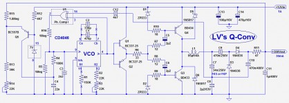
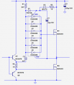
The circuit is unusual in that it uses a CD4046 PLL chip as a controller: it performs practically all of the required functions.
Power section:
The resonant circuit formed by L1 and C7 is driven by a PP of complementary transistors; the topology is not the ordinary follower, but a common emitter, more efficient at generating a rail-to-rail squarewave.
In order to achieve a fast and lossless switching, the driver circuit is rather special: it uses a double interlock mechanism allowing a safe and shoot-through-free switching without resorting to dead-times.
More on this later
The filter extracts the fundamental, and boosts it by a factor of ~25.
The resulting sinewave is applied to a voltage-doubler for rectification. In principle, the doubler shouldn't be necessary, but high boost ratios put very high demands on the reactive elements, and 25 is already hard enough. 50 would be almost unmanageable.
Control section:
The PLL is used almost normally, except it is locked to itself. This looks like an oddity, but is in fact quite useful:
The phase comparator compares the output of the VCO to an image of the current in the resonant circuit, sampled by C8.
C8 takes care of the quadrature imposed by the phase-comparator I.
As a result, the circuit will try to minimize the phaseshift between the output voltage and the current in the reactive elements, ie. drive them at the resonance.
This is quite useful, because it locks the VCO frequency to resonance of the passives, compensating for drifts and inaccuracies on both sides.
It also has another use: since the control is achieved by altering the balance, the sensitivity will be reduced by the gain of the loop.
Throwing control gain away in this manner may look counterproductive at first sight, but is in fact necessary: with a Q of 25, minute variations in frequency would cause huge variations of the output, making the stability control very difficult.
This mode of locking "dilutes" the control range, making it more manageable.
Regulator:
The regulator uses the internal zener and an external transistor: the emitter receives a fraction of the output voltage and compares it to the reference.
The collector generates an offset to the output of the phase comparator.
R5 offsets the initial point, allowing for a full dynamic range control.
To be continued...
Yet another HV converter? Maybe, but this one is rather unusual (as usual!).
It uses the Q of a tank circuit driven at, or near the resonance to boost the input voltage.
Such an approach offers a number of advantages:
- The resonant circuit being basically a high-Q second order filter, the output is a very clean sinewave, making the converter extremely quiet
- At the resonance, the switching occurs at the current zero-Xing, minimizing the switching losses
- The circuit is inherently overload and short-circuit proof
- The inductive element can be a regular 2-terminal choke; no need for taps or secondary
- The control strategy can be as simple as varying the drive frequency
Since there are two sides to every coin, there are less pleasant aspects as well:
- The reactive elements have to withstand severe stresses
- If the control loop is interrupted under light or no-load conditions, something goes BOOOM! -This converter is essentially a Norton generator-
These features make it ideal for supplying small tube circuits like preamps (<10W), and shunt regulators (which it can drive directly, being the ballast itself).
The circuit is unusual in that it uses a CD4046 PLL chip as a controller: it performs practically all of the required functions.
Power section:
The resonant circuit formed by L1 and C7 is driven by a PP of complementary transistors; the topology is not the ordinary follower, but a common emitter, more efficient at generating a rail-to-rail squarewave.
In order to achieve a fast and lossless switching, the driver circuit is rather special: it uses a double interlock mechanism allowing a safe and shoot-through-free switching without resorting to dead-times.
The filter extracts the fundamental, and boosts it by a factor of ~25.
The resulting sinewave is applied to a voltage-doubler for rectification. In principle, the doubler shouldn't be necessary, but high boost ratios put very high demands on the reactive elements, and 25 is already hard enough. 50 would be almost unmanageable.
Control section:
The PLL is used almost normally, except it is locked to itself. This looks like an oddity, but is in fact quite useful:
The phase comparator compares the output of the VCO to an image of the current in the resonant circuit, sampled by C8.
C8 takes care of the quadrature imposed by the phase-comparator I.
As a result, the circuit will try to minimize the phaseshift between the output voltage and the current in the reactive elements, ie. drive them at the resonance.
This is quite useful, because it locks the VCO frequency to resonance of the passives, compensating for drifts and inaccuracies on both sides.
It also has another use: since the control is achieved by altering the balance, the sensitivity will be reduced by the gain of the loop.
Throwing control gain away in this manner may look counterproductive at first sight, but is in fact necessary: with a Q of 25, minute variations in frequency would cause huge variations of the output, making the stability control very difficult.
This mode of locking "dilutes" the control range, making it more manageable.
Regulator:
The regulator uses the internal zener and an external transistor: the emitter receives a fraction of the output voltage and compares it to the reference.
The collector generates an offset to the output of the phase comparator.
R5 offsets the initial point, allowing for a full dynamic range control.
To be continued...
Attachments
Neat 🙂
The nice thing about a resonant converter is it's inherently short and open circuit proof; the output load line is 1/4 of an ellipse, without any added regulation (but tracking resonance).
The Z and Q seem suspect though...
Open, you've got L1 working into C7, which gives a resonant impedance of 53 ohms and "unlimited" Q (so you should have an inverter current limit function, in case the output ever goes nuts).
Shorted, you have L1 into C7 + C9 (and a little less due to C8; curious, why return C10 to C8 by the way?), giving 13.7 ohms and again a high Q.
Under nominal load, you have 10kohms DC, which is probably around 1/4 that or 2.5kohms AC. The tank impedance will be somewhere inbetween 53 and 13.7 ohms, giving a transformation down to 0.35 ohms let's say (Q = 85!), which will draw 17A, which I guess would be mostly reactive...
...That's probably an overestimate for the impedances under that condition. Of course there's no good formula for the average AC resistance of a rectifier. I think 1/4 Rdc is typical for half wave, so it's probably even less for half wave doubler.
Different ratios of C7/C9 would also give different operating curves. I don't know how optimal it is as shown, or what would be better.
Huh... aren't the zener diodes backwards, and/or drive applied to the wrong side of R9/R10..?
Tim
This is not a "regular" resonant converter, like a class E or normal ZVS: it is simplified to two reactive elements, which means there is no inherent mechanism to protect against open-circuit conditions. It is the resonant equivalent of a flyback converterNeat 🙂
The nice thing about a resonant converter is it's inherently short and open circuit proof; the output load line is 1/4 of an ellipse, without any added regulation (but tracking resonance).
It isn't quite a tracking converter: there is some tracking, but modulated by the controlThe Z and Q seem suspect though...
You could implement a crowbar circuit (zener + SCR or TVS), in case the feedback is interrupted. The problematic is similar to that of a flyback.Open, you've got L1 working into C7, which gives a resonant impedance of 53 ohms and "unlimited" Q (so you should have an inverter current limit function, in case the output ever goes nuts).
I preferred to monitor the actual inductor current; of course, I couldn't return the lower diode to C8 due to DC complications, but the first filter cap was OKShorted, you have L1 into C7 + C9 (and a little less due to C8; curious, why return C10 to C8 by the way?), giving 13.7 ohms and again a high Q.
The pivotal impedance is indeed around 53Ω at the "normal" resonance, but this normal case only applies at the maximal output power, and only when it is delivered in normal circumstances, ie with a 10K output load.Under nominal load, you have 10kohms DC, which is probably around 1/4 that or 2.5kohms AC. The tank impedance will be somewhere inbetween 53 and 13.7 ohms, giving a transformation down to 0.35 ohms let's say (Q = 85!), which will draw 17A, which I guess would be mostly reactive...
...That's probably an overestimate for the impedances under that condition. Of course there's no good formula for the average AC resistance of a rectifier. I think 1/4 Rdc is typical for half wave, so it's probably even less for half wave doubler.
At the resonance, the impedance seen by the drive is 53/Q, and the equivalent impedance (from an energetic point of view) presented by the rectifier is 53*Q
In all other cases, the Q is either much lowered, or not applicable because the drive frequency is very far from the resonance: this is the case for a short: the resonant frequency is very much lower than what the PLL limits allow (R1 sets the range) and the load becomes purely inductive, and completely recuperated by D5 and D6.
In case of a dead short, the measured supply current drops to 80mA, which is the driver consumption + the keep alive current for the rest of the circuit, including the power stage (less than 10mA in fact).
The maximum peak current in the transistors is ~3A, and occurs only at the nominal load (in case of an open output it would be much larger, but this is principle not allowed)
One could play a bit with these parameters, but the primary function of C9 is to provide energy storage for the doubler, and reducing its value means a higher voltage in front of the doubler, which is not desirable for a 300V outputDifferent ratios of C7/C9 would also give different operating curves. I don't know how optimal it is as shown, or what would be better.
No, everything is correct but will need some further clarification as I said, since it isn't obvious or straightforwardHuh... aren't the zener diodes backwards, and/or drive applied to the wrong side of R9/R10..?
Good stuff.
Have you had time yet to do any simple step load response testing, or step input voltage testing?
What do you think the efficiency is with that nominal 9W output and what is the likely percentage loss in to the transistors? Coud you have similarly used complementary power FETs?
Have you had time yet to do any simple step load response testing, or step input voltage testing?
What do you think the efficiency is with that nominal 9W output and what is the likely percentage loss in to the transistors? Coud you have similarly used complementary power FETs?
I haven't done these tests yet, but they are in the pipe...Good stuff.
Have you had time yet to do any simple step load response testing, or step input voltage testing?
I can already predict what the result will be in the case I have shown: the loop gain is very low (and the regulation is very poor as a result...), which means the step response will be very much like that of an unregulated supply: rather poor, but without artifacts or nasties.
The regulation accuracy (and the closed-loop nasties of course) can be increased by lowering the feedback resistances values, but I will come back on that later
For a 9W output, the input current is 1070mA, which translates into a 70% efficiency; not great by today standards, but for a moderately clean output, this is maybe a price worth paying.What do you think the efficiency is with that nominal 9W output and what is the likely percentage loss in to the transistors? Coud you have similarly used complementary power FETs?
The power lost in the transistors is very small: they just warm slightly.
Most of the losses occur in the inductor (that's up to you in fact: if you put lots of efforts into the design of this coil, the overall losses will become significantly smaller, but that's not necessarily sensible).
Complementary Mosfets could certainly be used, and in fact I had the intention of recommending Mosfets drivers as an alternative for lower power versions, but you overtook me 🙂
Here is an example of such a driver (I am sure better options are now available, this is just an example): http://ww1.microchip.com/downloads/en/DeviceDoc/21420d.pdf
This one cannot compete with the discrete version I proposed in spite of its 9A peak current capability, but for lower currents, it is certainly an option worth considering
I was thinking more of this type of part:
https://www.fairchildsemi.com/datasheets/FD/FDS8958B.pdf
but maybe shoot through can't then be easily managed.
What is the frequency span? Is the inductor a gapped PQ core?
https://www.fairchildsemi.com/datasheets/FD/FDS8958B.pdf
but maybe shoot through can't then be easily managed.
What is the frequency span? Is the inductor a gapped PQ core?
Their power characteristics are vastly superior to that of a complete driver. Of course, you need to do some homework to make them operate smoothly, but that shouldn't be too difficult compared to BJT'sI was thinking more of this type of part:
https://www.fairchildsemi.com/datasheets/FD/FDS8958B.pdf
but maybe shoot through can't then be easily managed.
In my prototype, the frequency span is 87 to 90KHz and the inductor is based on a planar PQ core that I gapped myself. Not a very good solution, because the gap needs to be large, half inside half outside, meaning atrocious stray fields (Ok, I could have tried to grind the center pillar, but I have the feeling it would have ended in a blood-bath).What is the frequency span? Is the inductor a gapped PQ core?
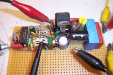
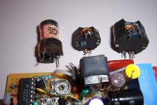
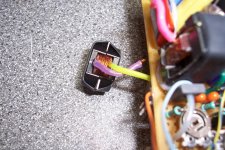
The inductor was the most difficult issue with this converter: I started with a standard power choke, based on a drum core, and it worked, but performances were not good.
I then opted for a custom-made RM6 based inductor. Material grade N67, copper window filled to the rim. It worked, but the iron became hot very quickly.
Next attempt was based on a RM8, N67 core, also with a good number of turns. This one worked quite satisfactorily, exceeding the expectations, the only problem was the bulk: it couldn't physically replace the previous ones.
In the end, I opted for this planar PQ core (N97 I think) with a self-supporting coil. No more problems of iron overheating either, but the huge gap made in an amateur way (with spacers) sent stray field everywhere.
During the first test, with the coil connected with flying wires, everything worked fine, like the RM8, but as soon as it was in its assigned place, things turned sour:the stray field interacted with the cans of the E caps, the foil of the PS caps and the metal tab of the TO126.
This reduced the efficiency and the maximum output power: in its present form, it only manages 290V out on a 10K load.
Here is an outline of the successive iterations:
Attachments
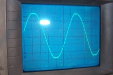
Here are one or two waveforms: the first is the PP output, on the collectors of the transistors.
Output power is maximal, which is visible because the Vcesat modulation is a perfect, well-centered arch, meaning the current is exactly in phase with the voltage.
Second pic is the filter output, just before the doubler. The tops are somewhat flattened by the recifier, but otherwise the general shape is that of a very good sinewave.
Nice thing with sinewaves: the rectifiers don't need to be blindingly fast as the rate of change of voltage is gentle.
The 1N4936 are "fast", but very ordinary: certainly not ultra-fast.
Attachments

I will now try to explain how the driver circuit works. It is a bit overcomplicated, but the end result is excellent.
Most of the series resistance for base current limitation is common to the N and P devices: R6 is much larger than R7 and R8.
Capacitors C5 and C6 take care of DC level issues, but not only: because each charge balancing diode D1 and D2 is equipped with a series resistance, the capacitors will end being charged at an average voltage > Vs/2.
This means that both devices will bend towards the Off condition. It is a first measure against shoot-through and simultaneous conduction, but not the only one.
Because the bases are tightly interconnected, and because of the bias, a transistor will only be able to conduct if the emitter junction of the opposite one has recovered completely from the forward conduction.
In other words, the drive for a transistor waits until the other has finished recovered.
Of course, waiting for emitter desaturation goes a long way towards a clean and ideal switching, but even when the emitter is desaturated, some carriers remain in the collector junction.
To allow for their evacuation, an additional time is provided by the reverse recovery of the base anti-parallel diodes: that is the reason for using zeners: unlike ordinary 1N4148, they aren't gold doped, and have a significant recovery time: around 150ns in this case. Because zeners must have a relatively thin junction to function, their trr is not quite as bad as ordinary Si diodes, like 1N400x.
Many years ago, it was possible to find GP diodes that were not gold-doped like the OA200 series or the 1N646, but today the simplest option is to use a zener (avalanche in fact).
The secondary delay provided by this diode only starts when the first one is cleared.
This timing sequence provides an adaptative delay, meaning no added dead-times and inherent temperature compensation: if the temperature increases, the collector desaturation time will also increase, but exactly in the same proportion as that of the compensating zener.
The result is near-perfect at 100KHz using slow transistors, and could certaily be pushed to 200 or 300KHz using the same devices.
Sorry for misdirection, I was thinking about the complementary powerMOS for the power half-bridge, not the driver.
Yes, small power inductors that need custom core legs are a pain for diy, and its frustrating when the datasheet shows a wide range of Al values but none are in stock. I'm sure there are many stories of how people ground the centre leg - sounds like you wanted quite a bit of grinding.
Did you go custom litz, or salvage from a commercial part, or ?
I used 5 strands of regular enamelled 0.23mm I twisted myself, but here with such a large gap, it was clearly suboptimal.Did you go custom litz, or salvage from a commercial part, or ?
Ideally, it should have been true litz, or at least 42 strands of 0.08mm. Maybe I'll twist them for my next attempt...
Design procedure:
Starting with the nominal frequency and the DC output power (voltage and current), first compute the Q or boost ratio:
It is the ratio of the peak output voltage before the rectifier and the fundamental component of the input squarewave.
In this example, the peak output voltage is 150V (because of the doubler), and the fundamental component is (12/2-0.5)Π/2.
The 0.5 is the saturation voltage of the transistors at high current, and the Π/2 is the value of the fundamental for an unity squarewave.
The theoretical Q is thus ~17.5.
To take into account the inevitable losses, this theoretical value should be increased by at least 25%.
Next step is to compute the equivalent AC load presented by the rectifier: convert the peak voltage into its rms value, and R=V²rms/Pout
Now, you can compute the characteristic impedance of the LC circuit:
Zc=R/Q
Since Zc=√(L/C) and F= 1/(2Π√(LC)),
L=Zc/2ΠF
C=1/2ΠZcF
The impedance seen by the squarewave generator is Zc/Q
The reactive elements must be suitable, ie have a Q much larger than the working Q, and they have to withstand the currents and voltages involved.
For the capacitors, there are only two practical alternatives (others exist, but they are too costly or too exotic): foil polypropylene or polystyrene.
Even a foil polycarbonate or a metallized PP would quickly meltdown.
The inductor has to have low losses, and this doesn't simply mean a low DC resistance: many other factors are of importance.
For relatively low power/low boost ratios, it is probably possible to use standard power chokes from Wurt or Coilcraft for example, but going higher requires custom coils.
It is important to bypass properly the DC supply: the ripple current is quite large. I have used a 100µF OSCON in parallel with a low-esr 470µF.
The DC input needs to be well regulated: the 4046 is sensitive to the supply voltage.
You will probably need to adapt the theoretical values you have computed.
When you first test the supply, be sure to load it with its nominal load.
To adjust R3, set R14 to 0Ω and adjust R3 for the maximum output voltage.
Once it is done, increase R14 to check that the regulation is working, otherwise do not remove the load until you have found the cause of the problem.
The regulation gain set by the impedance of the divider R13-R14-R15. With the values shown, it is very low, which means the regulation is loose: the voltage varies by a few volts between 0 load and the maximum.
It can be made tighter, but at some point there may be stability issues, depending on the Q.
To adapt the frequency, change the capacitors C1/C2, but keep the resistors value.
Note that for the 4046, there is a wide spread of oscillation frequency between manufacturers.
The schottky' across the transistors are not indispensable: they are completely inactive at resonance and serve only when reactive currents need to be recuperated; without them, there are alternative paths, but they increase the efficiency at loads < maximum
Hi Elvee,
I'm really lousy at switching type of project so please bear with me. Your Q-Conv got me interested because compared to other types of switching converter, resonant converter is supposedly quite low in EMI noise generation, your attention to detail and use of common easy to handle through hole components.
Perhaps you can give some pointers for me while I'm searching for more references :
1. When considering usage of a toroidal transformer, is it better to replace L1 or put the transformer in series with L1?
2. Is there any benefit in using vacuum tube rectifier for output DC rectification in terms of generated noise?
3. Also, would you recommend the use this design for low voltage AC filament supply? The problem is that I'm not sure of a reliable way to generate feedback. Would an optocoupler be recommended?
Thank you.
Let's look first at the transformer: you could replace L1 by a power choke+transformer combo, in essence a flyback transformer, except here it will work in sinusoidal regime, not pulse, but transformers are more or less agnostic.1. When considering usage of a toroidal transformer, is it better to replace L1 or put the transformer in series with L1?
However, this goes more or less against the spirit of this project, which in essence tries to avoid a full-blown transformer, but you are allowed to do it, of course.
If you simply replace the choke by a transformer, you won't reap the full benefits of the scheme though, from a quietness point of view: the inductor sees mostly a sinewave, but with the (smaller amplitude) squarewave input superimposed.
The completely clean and filtered output is only present across the capacitor.
You could place a transformer there, with the advantage that it only has to perform transformation duty, not energy storage. Of course, in this case, you will still need the choke, ie two inductive components.
Let's deal with the "toroid" part: for a simple coil, or a coil+transformer combo, no toroid alternative will work satisfactorily: toroids exist in ferrite or metal powders. Ferrite is unusable, because a toroid cannot normally be gapped, and a metal dust toroid won't work because of the high boost ratio, leading to excessive iron losses, even for advanced materials, sendust, MPP, etc.
Such toroids excell in more conventional topologies where their energy-storage capabilities are without equivalent, but here only gapped ferrite will work properly.
Even a standard drum power choke like the one I showed as example will work better than the best toroid.
If you use the second option (choke and transformer separated), you can use a ferrite toroid as transformer core.
I don't think there is any objective benefit to be had by using a "better" (faster, softer, etc) rectifier in this case: the source is completely capacitive, and cannot resonate in any way (unless you make a lousy work of the wiring).2. Is there any benefit in using vacuum tube rectifier for output DC rectification in terms of generated noise?
It can be seen in the voltage waveform I have published: even though the 1N4936's are crap by audiophile standards (not very fast, and not super-clean recovery), they produce no visible unpleasant artifact, for two reasons: the capacitive source I mentioned, and the sedate rate of change of current and voltage.
This is basically a high voltage, low current converter and going into the totally opposite direction is huge leap, but it is probably possible if you are determined to. However, I would first look at more sensible alternative, like using the 12V DC supply directly for example.3. Also, would you recommend the use this design for low voltage AC filament supply? The problem is that I'm not sure of a reliable way to generate feedback. Would an optocoupler be recommended?
From a general perspective, this circuit operates as an impedance transformer, and in principle it could go from high to low too... but as always, the devil is in the details
I have developed an alternative power stage based on MOSfets, but this one uses only N-channels, which are cheaper, more efficient, and exist in a wider variety than P-types.
The job of inversion/bootstrap for the upper device is carried out by an IC, but it is again a commodity, an hex CMOS inverting buffer.
An ordinary 4069 hex inverter also works, but the 4049 gives slightly better results.
As a result, the efficiency of the converter is somewhat improved because the driver's consumption is reduced (~1W for the Bjt version), and because the squarewave swings closer to the supply rails.
Attachments
Hi Elvee, you are so kind giving good and conscise guidance. Many thanks. 
Some background. For quite a while I have been searching for sinusoidal (to minimize potential noise problem) HF HV DC supply and HF LV AC filament supply for a compact DHT hybrid amplifier. So far the alternatives I found require SMD parts which I am hesitant to use. Very happy you decided to share the Q-Conv which generate 150V sinusoid at 90kHz, just what I need.
I'll first build it as designed but without the doubler. I can get gapped ferrite EI core for L1, if that does not work I know how to make a gap on ferrite toroid by using a hacksaw and mini grinder. I'll tinker with the transformer for galvanic isolation later. I hope I'll be able to get the adaptations I want well enough.
If you have the choice, try to use a modern, high performance ferrite material: for example, 3C98 in the ferroxcube system or N49, N97 for Siferrit.I'll first build it as designed but without the doubler. I can get gapped ferrite EI core for L1.
Standard power materials like N41 won't work well.
Even with "good" ferrites, stay below 150mT^ induction, 100mT^ is even better if you're not space-constrained.
For the winding, use preferably litz wire, or at the very least multistrand.
Do not be too generous with the current density: this may look paradoxical, but since eddy current losses are the dominant factor for this kind of inductor, reducing the bulk of copper to the strict minimum is beneficial
In the end, I managed to pack the inductor into a RM6 core: I used N49 material with a self-supporting coil, allowing for a bit more turns.
The peak induction is 210mT, and the iron only heats up mildly.
The only issue with this choke is the wire: too few strands for the section, but the temperature rise remains bearable, and with this choke, the converter has no problem reaching 300V and beyond into its 10K load.
With proper litz wire, it should work even better. That will be the next step
Attachments
Do you recall what was the peak voltage across the winding and the peak between two turns on different layers? As it is a sine current, with low harmonics, what wire diam would want for skin depth.
The total voltage is 150V^, and there are 37 turns in 5 layers (some 7, some 8).Do you recall what was the peak voltage across the winding and the peak between two turns on different layers? .
Maximum voltage between two turns is therefore for 8+8=16t, about 65V
Skin effect is not really a problem here, even with 0.23mm: the skin depth is 0.2mm, and Rac~=Rdc to one percent or thereabout.As it is a sine current, with low harmonics, what wire diam would want for skin depth
The DC resistance of the winding is 100mΩ, and based on Joule's effect only, it should dissipate 0.4W (Irms=2A)
But the actual dissipation is about 3 times as much, and the eddy currents are to blame.
This is a problem common to all inductors subjected to a large reactive power: 215VA here. If even a small proportion of this power is lost, it immediately translates into a significant, real and active power dissipated.
The only remedies are distributed airgaps, or finely divided wire
- Status
- Not open for further replies.
- Home
- Amplifiers
- Power Supplies
- A small resonant HV converter: Q-Conv