No, I think you have an older model, with parts changes. The A relates to the size and configuration of the power supplies. The B is a mod to have the unit non-invert in overall operation, and we call it 'Harry proofing' the design. The C mod replaces second stage mosfets with high Idss 2SK147-J72. and gives 10 times lower distortion (put that in your simulation and find it). The D mod changes out the mini 1A diode bridges (4) with 16 discrete hi speed diodes, for lower RFI generation. The T mod swaps Teflon for polystyrene in the EQ caps. There is one more mod sometimes made, called the G mod, which adds about 10 dB gain by changing the Eq values. I also have added a P mod that swaps out the Vendetta power supply boxes for CTC power supply modules. I don't do these mods very often or with much relish, but I like to help people who really care to have the best that I can supply.
Last edited:
John,
Can a very dextrous DIY'er perfom the mods himself? Asking because I've developed my skills abit.... and I'm an original owner of an "A" I bought in the mid 80's (from Victors in Chicago.. now long gone) and had you upgrade it to a "B" in the late 80's. Still love the beasty 🙂 still performs flawlessly.
Jeff Davison
No, I think you have an older model, with parts changes. The A relates to the size and configuration of the power supplies. The B is a mod to have the unit non-invert in overall operation, and we call it 'Harry proofing' the design. The C mod replaces second stage mosfets with high Idss 2SK147-J72. and gives 10 times lower distortion (put that in your simulation and find it). The D mod changes out the mini 1A diode bridges (4) with 16 discrete hi speed diodes, for lower RFI generation. The T mod swaps Teflon for polystyrene in the EQ caps. There is one more mod sometimes made, called the G mod, which adds about 10 dB gain by changing the Eq values. I also have added a P mod that swaps out the Vendetta power supply boxes for CTC power supply modules. I don't do these mods very often or with much relish, but I like to help people who really care to have the best that I can supply.
Thanks John, much appreciation. Can you provide any how to docs / parts list or priide a parts "Kit"? If you need me to send you the serial number let me know.
... btw all.... sorry for the thread hijack.
Jeff
... btw all.... sorry for the thread hijack.
Jeff
Some mods you can do, some are difficult to get the parts for.
No, I think you have an older model, with parts changes. The A relates to the size and configuration of the power supplies. The B is a mod to have the unit non-invert in overall operation, and we call it 'Harry proofing' the design. The C mod replaces second stage mosfets with high Idss 2SK147-J72. and gives 10 times lower distortion (put that in your simulation and find it). The D mod changes out the mini 1A diode bridges (4) with 16 discrete hi speed diodes, for lower RFI generation. The T mod swaps Teflon for polystyrene in the EQ caps. There is one more mod sometimes made, called the G mod, which adds about 10 dB gain by changing the Eq values. I also have added a P mod that swaps out the Vendetta power supply boxes for CTC power supply modules. I don't do these mods very often or with much relish, but I like to help people who really care to have the best that I can supply.
Thanks John for your account with us! I greatly admire that!
But now I came two questions:
1) In the second stage of C mod you replaced all the mosfets by fets or just the mosfets gain and keeping the cascode mosfets?
2) Which way is the Vendetta configured to operate in a non-invert (I don´t know "Harry proofing" design - is some kind circuit's topology?)
regards
eD
'Harry proofing' is a pointed criticism of Harry Pearson who once reviewed the product, ignoring the polarity inversion, and wondered why his favorite records sounded somewhat different. Gave me a bad review, mostly because of it. The B mod double inverts to give a total non-inverting output. It is too difficult for amateurs to do this with existing boards, so I recommend that you stick with the A mod, that you have now.
Keep the cascodes as mosfets.
Keep the cascodes as mosfets.
Last edited:
'Harry proofing' is a pointed criticism of Harry Pearson who once reviewed the product, ignoring the polarity inversion, and wondered why his favorite records sounded somewhat different. Gave me a bad review, mostly because of it.
"Harry proofing" ... I love it!! 😀
Mind you, I can't understand why designers produce a circuit which does invert ... when it's so easy to add another stage to turn it back to "straight-through". I have a head amp designed by Hugh Dean (AKSA) and, while it's a brilliantly executed design, it really pisses me off that I have to swap cartridge connections when I change to another phono stage which doesn't need a head amp before it. 🙁
Regards,
Andy
Sometimes, it is not as easy as you think, especially when designing a world class preamp.
Fair enough. 🙂
Regards,
Andy
'Harry proofing' is a pointed criticism of Harry Pearson who once reviewed the product, ignoring the polarity inversion, and wondered why his favorite records sounded somewhat different. Gave me a bad review, mostly because of it. The B mod double inverts to give a total non-inverting output. It is too difficult for amateurs to do this with existing boards, so I recommend that you stick with the A mod, that you have now.
Keep the cascodes as mosfets.
Thanks John,
if I did understand well, you use the second stage as inverter mode, resulting in general non-inverter mode at the end as the first stage is inverter too.
eD
That's right, but it is not easy with existing boards. There are some servo interaction problems, as well. For an individual, it is probably best to stick with an A, if that is what you have.
Ok John,
but if we have the best of the versions would be a prize for us. From the moment you say that there is a better version, we create an expectation of achieving it. After all, we are expending efforts to complete one of the versions, so why don´t do it with the best of them (if you allow, of course). I know you understand us now, otherwise you would not do what you do. These are things that drive us to get even more for self satisfaction.
I would like to do some simulations taking into account the changes you suggested to us and present the results here but I'm out of time this season. I'll be on vacation in January and so yes, I think I can do that. Until then, making slow progress.
Regards
eD
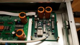
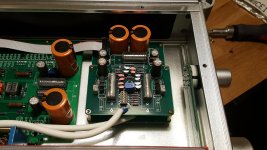
Interesting thread. Did anyone actually build the amplifier - except John himself of course? ��
Maybe I'm the first?
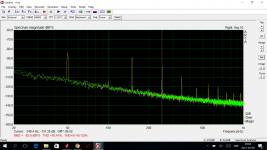
Yellow trace is preamp on top of power supply.
Green trace is preamp moved some distance away.
~80dB at 50Hz is quite sensitive for stray fields...
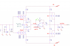
This is not quite what is the describe in the schematics in this thread tough.
Yellow trace is preamp on top of power supply.
Green trace is preamp moved some distance away.
~80dB at 50Hz is quite sensitive for stray fields...
This is not quite what is the describe in the schematics in this thread tough.
Attachments
Last edited:
🙂
The gain is very good!
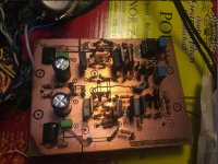
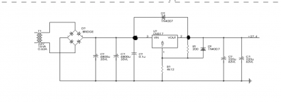
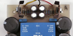
There is a problem ! There is a direct current at the start! A few seconds of a 19-volt DC then drops to 0.050.
I think the problem is in Chinese details = all parts are fake!
BUT IT PLAYS !!!!!)))))
How to overcome the problem!? I do not know
I can not understand why the AD711 chip is powered by 20 volts
schematic -EDDELARUE
The gain is very good!
There is a problem ! There is a direct current at the start! A few seconds of a 19-volt DC then drops to 0.050.
I think the problem is in Chinese details = all parts are fake!
BUT IT PLAYS !!!!!)))))
How to overcome the problem!? I do not know
I can not understand why the AD711 chip is powered by 20 volts
schematic -EDDELARUE
Attachments
Last edited:
There is a direct current at the start! A few seconds of a 19-volt DC then drops to 0.050.
Try disconnecting the servo, to see if it still does that.
Is the output of the servo attenuated by two resistors?
1- I disconnected the capacitor from the circuit (green). The direct current of 2 volts on the first board and 21 volts on the second board at the output stood and was.
2- I removed two chips — I removed it completely from the board. DC 2 volts on the first board and 22 volts on the second board --- standing! was!
3- I put the microcircuits back --- in two minutes it slowly fell and came 50 mV. on first. and 50 mV to the second. in two minutes
4- if you measure the voltage -
1- to the mass of the input first contact + output (second board) = 20 v DC
2- the mass of the main power + output 50 mV
connect sound to the amplifier - great sound
Attachments
-
 ?????? ?????? 2019-07-10 ? 12.56.56.png243.6 KB · Views: 479
 -
 ?????? ?????? 2019-07-10 ? 13.08.39.jpg280.9 KB · Views: 304
 -
 ?????? ?????? 2019-07-10 ? 13.08.33.jpg248.4 KB · Views: 188
 -
 ?????? ?????? 2019-07-10 ? 13.08.21.jpg327.2 KB · Views: 177
 -
 ?????? ?????? 2019-07-10 ? 13.08.16.jpg274.6 KB · Views: 165
 -
 ?????? ?????? 2019-07-10 ? 13.08.09.jpg310.9 KB · Views: 204
Last edited:
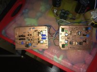
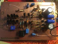
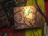
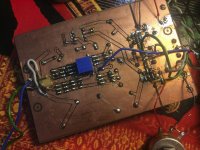
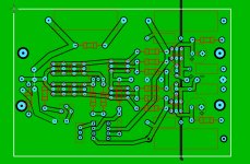
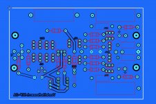
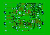
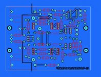
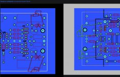
With fake parts it is not possible to build low noise phono preamps. You may attach PCB artwork for diy PCB-s for us who have genuine Toshiba J-Fets, to try.
🙂
1-I'm not greedy - please- I used the schemes
EDDELARUE
2-The circuit direction of the transistors (some) is not true! carefully watch the diagram EDDELARUE
(or my photos)
3-power board remade for power scheme (there is a difference with the original photo!)
Hopefully with the original parts, this should work well! 18 volt power supply
I will wait for the results of repetition
I hope the AUTHOR of the SCHEME JOHN CURL (original) will not be offended! I took photos of boards on the Internet!
Attachments
-
 ??333????.JPG205.2 KB · Views: 196
 -
 ????4444??.JPG189.2 KB · Views: 187
 -
 ???222???.JPG198.1 KB · Views: 182
 -
 ????111??.JPG180.9 KB · Views: 192
 -
 ?????? ?????? 2019-07-10 ? 13.58.19.jpg206.9 KB · Views: 176
 -
 ?????? ?????? 2019-07-10 ? 14.00.59.png63.5 KB · Views: 211
 -
 ?????? ?????? 2019-07-10 ? 14.00.40.jpg109.2 KB · Views: 216
 -
 scp-2a-h.jpg125 KB · Views: 192
 -
 ?????? ?????? 2019-07-10 ? 14.13.56.jpg219.3 KB · Views: 183
Last edited:
- Home
- Source & Line
- Analogue Source
- A real Vendetta?