Except for the string of diodes these circuits are similar to what Borbely has been doing for years.
> Another non usual topology. What does it do?
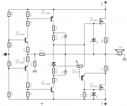
Makes 50 Watts in 8Ω. Good if you can hear 1MHz.
T1-T8 run Class AB. They give voltage gain to the FET Gates. Source resistors unbalance the current mirrors.
I can't jot the bias or performance without knowing the properties of R17 R18. ("3cm resistance wire..." isn't enough.) But guessing:
At high current the whole T1-T10 chain runs in transconductance mode: input voltage sets output current. Special features are that: Beta can be very low, meaning performance is little changed up to nearly Ft; FET Gate capacitance is strongly driven and does not dominate response inside the audio band. Somewhere above 1MHz the declining Beta and Gate impedance makes the whole thing run out of steam quickly.
How can T3 and T4 form properly current mirror, if one has R17, and the other has emitors straight to rail?
I read that this topology has a "non-turnoff" property for final transistors. Always on, although it do not run in classA. How to trace this non-turnoff in this cct?
I read that this topology has a "non-turnoff" property for final transistors. Always on, although it do not run in classA. How to trace this non-turnoff in this cct?
lumanauw
this 2 diodes seem to be not enough for 2 times Vbe voltage drop, so the input stage may work (depending on transistors) in push pull class A through AB, B to C.
you MUST use more diodes vith bjts in diffy..
also it seems hard to adjust biasing and nothing seems to preserve output mosfets fromturning off.
Also the purpose of opamp is ?????
I don't understand it - it is weak or as brilliant as I cannot imagine
> How can T3 and T4 form properly current mirror, if one has R17, and the other has emitors straight to rail?
I did say, didn't I, that it was "unbalanced"? Mirror ratio is 1:1 minus a function of output stage current. This gives negative feedback. It appears that output stage current is a function of error voltage. Also the unbalance vanishes at small output stage current, so the output devices are not driven hard-off.
> this 2 diodes seem to be not enough for 2 times Vbe voltage drop
Another (poor) current mirror. ASSuming that junction size is similar, diodes and BJTs (approximately type for the types specified) then T1 T5 current is similar to D1 D2 current. D1 D2 current can be trimmed with RV1 RV2. I assume these are trimmed for some small voltage across the 10 ohm resistors.
> the input stage may work (depending on transistors) in push pull class A through AB, B to C.
It will never run Class C (except in gross overdrive) and won't stay in Class A well. It is clearly intended to run in Class AB, probably with a few dozen milliVolts across the 10 ohm resistors at idle, and maybe 50mA peaks to whang the FET Gate capacitance.
> the purpose of opamp is ?????
The output stage T1-T10 makes good power and bandwidth, but has low and very variable input impedance, wide swing in input current, and voltage gain around 5. THD is low for a power stage but higher than we might want. DC error is non-negligible. For a complete hi-fi amp we want more gain, higher impedance, and (in best 1980 thinking) more global feedback. The opamp does that.
> i think R17 ,R18 give a temperature stable for mosfet.
FET tempco is completely inside feedback. Output stage hot-up can't cause thermal runaway. RV1 RV2 offset the BJT quad which forces a correcting offset across R17 R18, fixing output bias current. The BJT quad has large tempco which is first-order corrected by diode tempco. Diodes and BJTs should be thermally coupled.
tak, niestety bóg uczyni³ mnie Polakiemdarkfenriz said:witaj padamiecki rodaku
tak, jak moje!!!darkfenriz said:nietety moje projekty zwykle koñcz¹ swój ¿ywot na kartce lub w spicie 🙂
jeœli ³adnie gra, to mogê siê do³o¿yæ do p³ytki (jeœli gdzieœ je zamawiasz?) i zamówiæ na wersjê stereo, bêdzie taniej.aktualnie jeden cierpliwie oczekuje na p³ytkê..
By the way, the design sent by Steven is realy fine
darkfenriz said:hi steven
the schematic you attached is GREAT for me but not high input impedance I fear, yes?
Correct. Input impedance will be determined by the input series resistors because of the shunt feedback.
Steven
I would give a buffer/opamp then and small series resistors to minimize thermal noise of feedback substraction
regards
regards
It's an output stage, so noise of the input resistors is normally not a problem at these levels. You can take 10k input resistors to get a reasonable input impedance and still low noise.
Steven
Steven
"not low" means is high 😀 .darkfenriz said:thanh
how do you mean 'not low'?
could you attach the same in log scale
frenquency or Voo in log scale ? i will try to do it🙂
darkfenriz said:hallo
Have you ever used (or considered😀 ) something like this ?
seems to cancel some distortion compared to CFB, doesn't it?
Yes, except that I do not use D3-D10, but have 100R from the feedback point to rach LTP transistor, and 100R from input to each LTP.
The basic idea is the same, though, and it works great for me. 😀
Jennice
- Status
- Not open for further replies.
- Home
- Amplifiers
- Solid State
- A push-pull differential stage- why not?