I'm not sure what caps you mean, or how you think they remove gain. You're going to have to be more specific if you want to contribute positively to this thread.
I chose not to use a CCS in the VAS, and probably won't unless it shows significant improvement to the design in simulation.
By my standards it is an over complicated amplifier.
There seems to be a lot of capacitors slugging transistors from c to b.
Whats the point of adding extra gain then slugging it ?
The bias cct needs a ccs to keep the voltage across the bias cct the same or it will fluctuate with signal.
My amps use a 7 transistor driver and that includes ccs on the bias/vas stage.
Be careful of othrrs opinions because you will end up with dozens of unnecasary transistors in your design.
Remember the old addage KISS (keep it simple)
Dozens of transistors will probably work but will be a nightmare to debug.
By my standards it is an over complicated amplifier.
If you think this one is complicated, you should see mine.😀
There seems to be a lot of capacitors slugging transistors from c to b.
Whats the point of adding extra gain then slugging it ?
The only capacitor that will 'slug' GBW is the phase lag (Miller) compensation of C4. It's function is to set the dominate pole frequency, i.e. reduce the gain as the phase reaches toward 180 degrees and the then positive feedback oscillates the amp.
Q14 &16 should have a rather constant conductance (none or very little) except when there is over-currrent in the OPS. You might add a cap across the Vbe multiplier, but you don't want it too big. I'd say about what Self used would work. This cap will provide AC coupling between the bases of the drivers/OPT. The Z of this cap decreases as frequency rises and this helps compensate the fact that as frequency increases it takes more current to suck the minority carriers out of the base/collector depletion region of the BJT in order for them to turn off during the zero output current crossover region and prevent cross-conduction.The bias cct needs a ccs to keep the voltage across the bias cct the same or it will fluctuate with signal.

If, for example, someone decided to take this design, bump up the rail voltage a little, (of course then you might as well regulate it.🙂 ) for the input and VAS stages, then add cascodes to both the input and VAS, you would consider this a complication that yields no benefit?Be careful of othrrs opinions because you will end up with dozens of unnecasary transistors in your design.
FACT....common base amplifier (cascode) makes a much better VAS than common emitter. But you pay for it with a little extra complexity.🙄 There is never really a free lunch...
I suppose implementing a 2 pole compensation scheme, to increase usable GBW, would be considered too complicated.

BTW, you could always reduce 1 transistor, 2 resistors, and a cap by replacing the BJT ring CCS for the input stage source with a self bias J-fet.😉
True adage, but simplicity is relative.🙂Remember the old addage KISS (keep it simple)
Dozens of transistors will probably work but will be a nightmare to debug.
PS: What would happen if the bias pot wiper were for some reason or another to break and become open?
It may be possible some of the magic smoke might leak out of the circuit.😛
You might want to address this when you build the real physical amp as simulated pots don't break...
Last edited:
Thanks for your suggestions. I think I asked about the cap across the Vbe transistor earlier. Makes good sense to include it; thanks for the explanation. Should it go across the entire bias circuit like Self's Blameless, or just across the transistor itself, like Leach? Also, I'm thinking the cap sometimes used, across R15 in my amp, could be added for similar reasons? The "Speedup Switchoff" cap in the Blameless.
I think I also mentioned adding a resistor in series with the pot wiper. I wasn't sure if it was needed or not.
I think I also mentioned adding a resistor in series with the pot wiper. I wasn't sure if it was needed or not.
Is this your first amp?
My experience with CFPs is that the outputs can easily go deeper into saturation than with an EF and this leads to sticking, cross-conduction, and potentially oscillation due to the output stage pole shifting. It is said that an EF stage cannot go into true full saturation. Your stability analysis will probably be based on a small signal model. R33 and R34 help to limit the drive to the outputs, but are not a complete solution. I've been planning to try the newer faster output devices, but do not know when I'll have the time. These may lead to a greater tendency for local oscillation, which CFPs are known for, but I'm not sure, would probably have room for base stoppers just in case.
My experience with CFPs is that the outputs can easily go deeper into saturation than with an EF and this leads to sticking, cross-conduction, and potentially oscillation due to the output stage pole shifting. It is said that an EF stage cannot go into true full saturation. Your stability analysis will probably be based on a small signal model. R33 and R34 help to limit the drive to the outputs, but are not a complete solution. I've been planning to try the newer faster output devices, but do not know when I'll have the time. These may lead to a greater tendency for local oscillation, which CFPs are known for, but I'm not sure, would probably have room for base stoppers just in case.
Technically the current feedback pair has voltage gain (Av), thus it has a pole that as you mentioned can shift around. Also the CFP and stability is more related to load Z than EF as the output is taken from the 'dependent current source' of the transistor, the collector.
The wiper of the bias pot should connect to the emitter of Q8 and the base should connect between the top leg of the pot and R11. This way if the wiper becomes open then the output stage bias is cut off resulting in a lot less damage.😉
The Vbe cap should connect between the bases of Q9 & 10. R27 is essentially part of Q8.
It only has voltage gain, if the feedback is designed that way. Do you mean at RF when stray inductance is taken into consideration?
Is the Av not unity? Maybe, I could be wrong and unity gain nullifies that issue.😕 Any CFP experts out there could shed some light about this?
If the feedback node (of the CFP) is connected to the output load, do you think the squirrelly impedance of a speaker might have effect on that local loop? It may not have such a significant effect as it would if the output stage had CL gain. I am not an expert on CFP per say, but I have toyed with it some. I have seen the CFP used to drive a final follower stage. What do think of this idea?
I would think RF injected somehow into this fb loop could cause instability. Faster transistors would naturally make it more sensitive to this I suppose. 🙄 I suspect that PCB layout in this area would also have an effect on stability.
Last edited:
Hi,Here it is. Protection circuit is a complete rip from the Low TIM Leach. I think everything is good now; I still need to figure out how to calculate C3 and C5 Fc points, though... And simulate, prototype, build, etc...
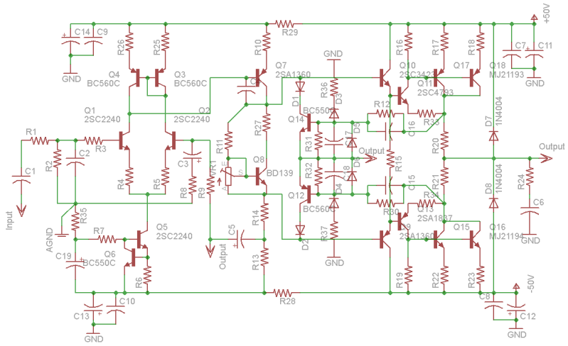
The Leach protection is a two slope current limiter.
He has not included the extra resistor that is required to monitor the Vce of the output device and thus achieve IV limiting.
You get much better protection into reactive loads with the extra resistor.
How about disconnecting all the protection/limiting while in the simulator and getting the amplifier to give you understandable answers to the questions you ask of it.
When the amp is doing what you can understand, turn stages of the limiters back on and start investigating what each component value does to the output and to the internal components.
Last edited:
Yes, this is my first design, but not my first project and it will not be my first time doing a pcb layout. With guidance, I'm sure I could get this design to work reliably, but it almost seems like extra trouble using CFP for no real gain over EF. Reading the "P3a Oscillation" thread it seems like I should use slower devices (MJE15034 drivers, etc...) to keep it stable, going by what AKSA and others have said there; especially since I plan on using slow outputs, MJ21193/94. If I changed my intended layout and added another pair of outputs (three pairs total) I could switch to the faster MJL4281/4302 outputs, allowing me to use better drivers (2SA1837/2SC4793). This isn't entirely important to me though, the MJE/MJ parts would do perfectly fine.
As far as layout goes, if the drivers need to be as close as possible to the outputs, then TO264 plastic parts would be better than the TO3's i had planned. And, the drivers need to be on a heatsink with Q8... Seems like CFP isn't very convenient for more than one pair of outputs. The board needs to be single sided to make it easier to prototype. I plan on building one channel just to confirm proper operation in real life, and to torture it.
All of this is making me lean towards a basic, triple EF. So far, the only positive writings I've read on CFP have come from Rod Elliot. I've read alot of negativity towards it here. I'm sure part of that is from inexperienced builders (like myself) jumping into it and expecting it to work the first time off the bat, with little effort. Given my goal of a stable, reliable amp, is there any scientific reason why I should stick with CFP?
Last edited:
You have a good scope I take it?
Do you have a lab split power supply with current limiting?
No reason not to do it if you like a challenge, and since you are prototyping you can always switch to EF if things don't go well.
Do you have a lab split power supply with current limiting?
No reason not to do it if you like a challenge, and since you are prototyping you can always switch to EF if things don't go well.
You have a good scope I take it?
Do you have a lab split power supply with current limiting?
No reason not to do it if you like a challenge, and since you are prototyping you can always switch to EF if things don't go well.
Not really a good one, but I have a 15Mhz Hitachi that works most of the time. I have access to 100Mhz analog and digital Tek's if I really need one. I do have a good lab power supply. By the time I start the physical work on this I should have a better scope.
I'll keep trudging forward with this scheme then. Thanks for the help everyone, as always.
My bad, i didn't see that as it's kind of difficult to make out the miller caps number buried in the Vas transistor 😀C5 is the bootstrap capacitor, 100pF would be a bit small there. 😀 C4 is the miller comp cap; 100pF would be appropriate there.
Interesting thread. Syn08's post seems like another nail in the CFP coffin for me. I'll probably decide either way when I start simulating the design, but I'm going to draw up another diagram of this design with an EF output stage and post it for approval/improvements.
Hi
When you build the physical circuit, you might only build the input stage and VAS, leave out the output stage at first. Then build on two seperate PCBs (I assume this is a vero-board like prototype) one with the drivers and EF, the other with the drivers and CFP. This way you can switch between them and see how each works out. Start with the EF as it is much simpler. Just a suggestion.
When you build the physical circuit, you might only build the input stage and VAS, leave out the output stage at first. Then build on two seperate PCBs (I assume this is a vero-board like prototype) one with the drivers and EF, the other with the drivers and CFP. This way you can switch between them and see how each works out. Start with the EF as it is much simpler. Just a suggestion.
I've started modeling in LTspice using Onsemi models (MJE340/350 VAS and drivers, MJ21193/94 output models), and LTspice BC546/556 models for the input stage. I'm just using these to get started. I've got the basic schematic loaded in, no protection circuit, and it seems to work. I've ran a few simulations on it but I guess I'm not sure what I should be looking for to confirm I have a stable design. I ran an AC analysis sweep, and found (no surprise) with no miller comp cap across the VAS transistor there is a ~4db peak in the response at ~700Khz. With a 100pf miller comp cap it goes away and response is flat out to 100Khz...
I need to read a lot more about simulation with LTspice, but I'm making progress. I don't think learning how to add models, navigate the menus, and do some basic sims is too bad for an hour or two of plugging away at it. 😀
I need to read a lot more about simulation with LTspice, but I'm making progress. I don't think learning how to add models, navigate the menus, and do some basic sims is too bad for an hour or two of plugging away at it. 😀
Last edited:
The sims I did in this thread have SPICE directives for distortion measurement. Then I also do sims for loop gain, and open loop gain:
http://www.diyaudio.com/forums/solid-state/163616-spice-simulation-adcom-gfa-555-a.html
Drive it hard with some clipping at 10 or 20 KHz, look at the VAS output, currents in the outputs, etc. Diff pair voltage and current.
Short the output and look at the currents when you drive it hard, leave out the current limiting to start.
Last time I tried those outputs, which was probably 2 or more years ago, they did not work well in clipping if I remember correctly - not sure but keep it in mind if you see anything strange. I lean toward Fairchild models, the ones I use in the Adcom seem to work well so far, I have not done extensive testing.
Last edited:
The Slone is a CFP with fast output devices, really is a Self Blameless. Excellent debugging here by 5th Element:
http://www.diyaudio.com/forums/solid-state/160061-slones-11-4-blameless-2.html#post2063936
http://www.diyaudio.com/forums/solid-state/160061-slones-11-4-blameless-13.html#post2100053
http://www.diyaudio.com/forums/solid-state/160061-slones-11-4-blameless-2.html#post2063936
http://www.diyaudio.com/forums/solid-state/160061-slones-11-4-blameless-13.html#post2100053
Short update:
I'm still working with LTspice and modifying the design as I learn. One thing I'm thinking about now is whether to use a current source for the VAS or stick with the bootstrap. I know there are varying opinions on using a CCS vs. bootstrapping the VAS, and I'm not sure where I stand quite yet. I haven't found any solid info on the pros of bootstrapping besides some saying it subjectively sounds better, which doesn't get it for me. Thoughts?
I'm still pondering EF vs. CFP, and probably will be until I actually get to build and test this.
- Status
- Not open for further replies.
- Home
- Amplifiers
- Solid State
- A "Patchwork" Type Concept Amp