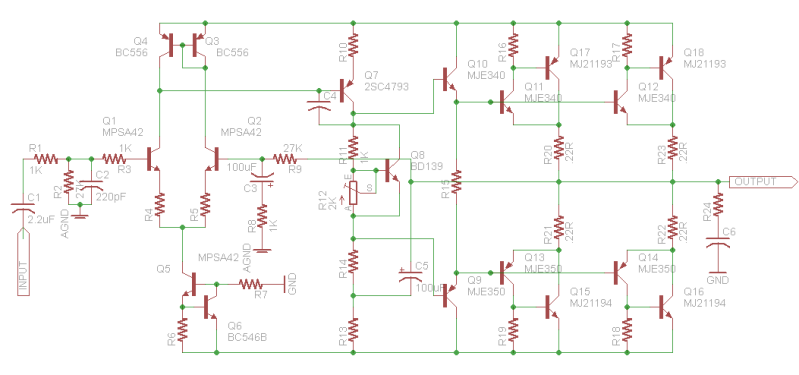
Here is an idea for a circuit i drew up. It's nothing new, just a few things I "patched" together. My own "patchwork" amp of sorts. The output stage is dual (?) CFP, which I saw a sketch of posted by Event Horizon in a thread recently. Input stage is mostly P101, and the VAS is generic. There will be an RC filter for the front-end, and bypass caps for the output stage; I just left them out to keep the diagram simple at first. I'm also thinking about adding VI limiting.
This is merely a concept drawing.
I haven't figured out LTspice yet, so I'm awaiting that to see if this will even work, and to figure out the component values. Some are already filled in with arbitrary values.
I'm looking for ideas, but take it easy on me. This is my first, albeit pseudo, design. If it looks good, I'll be looking for device suggestions for the frontend, VAS, pre drivers, and drivers. I'm thinking +/-45Vdc to +/-55Vdc rails with two pairs of MJ2119X outputs.
Last edited:
this type of output has been presented in the past in the forum by another greek member .... The person who designed this, claimed that topology with one driver per one output transitor had amazing drive ability and actually forced outputs to their best ... ( very good amp for wierd or watt asking loads )
in practice when he brought his amp to the shop it prooved that had very limmited bandwidth to preserve stability and other than that was an oscilation nightmare ...
not to mention a gozillion millers/snubers here and there to stop oscilations that actually managed up to a point but killed all amplifier sonics
so yes ...it looks like a very nice idea but the trick is to find ways and pcb to keep both stability and bandwidth while oscilation free ...
not an easy task ....
Last edited:
Well, if the CFPs really make problems you can always hack the board to emitter follower outputs 😉
Have fun, Hannes
Have fun, Hannes
Hi,
excluding the CFP, which I cannot comment on, I'll start at the front.
Add a DC blocking cap. Select it to set the bass passband. All other bass limitations in the amplifier must be of lower frequency than this HP filter.
Change the MPSA42 in the LTP. You need high gain, high frequency, low Cob, adequate Vce0, flatish gain with Ic.
Add degeneration resistors to the current mirror.
Adjust the base current of the VAS to match the total base currents of the two mirror transistors. (it took me 40years and the help of GK to realise this).
Q3, 4 & 6 do not need to be the high Vce0 version. bc550c/560c would be better here. Similarly Vbe multiplier does not need medium power device. It is only used for the convenience of having a fixing hole in it.
Change the VAS transistor from a driver type to a more suitable device., eg. 2sc3423
Add D.Self's resistor to the Vbe multiplier. Move the driver base to the Vbe collector. Add in the extra resistor between the top of R11 and the base of q10. This is particularly useful when the VAS is not supplied with a constant current. The Vbe likes to see a constant current and Self's resistor increases the tolerance to small changes in Vbe current.
C3 & C5 must be adjusted pro rata with the DC blocking cap.
Change Q9 & Q10 to more suitable devices, these pre-drivers could be same spec as the VAS
Relabel the output resistors. Your .22r looks like 22r and should read either 0.22r (never omit the leading zero) or 0r22, then there is no possibility of confusion.
Connect the signal grounds together. RCA ground PCB input ground, NFB ground, RIn resistor ground, RF filter cap ground.
Where should r7 ground go?
Taken to the signal ground and it adds a dirty current to the clean side.
Take it to the decoupling/Zobel ground and it gets contaminated by the horrible pulsed currents around there.
Taken to the +ve supply rail and decoupled back to the -ve supply rail? Is that too elaborate?
Do not take the NFB tapping to R9 from the output resistors. Take it from the single line out to feed the Zobel circuit.
read thread
http://www.diyaudio.com/forums/solid-state/164116-p3a-oscillation.html#post2136099
Last edited:
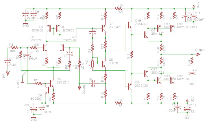
2SC2240 look better for the LTP.
As you said, the Vbe multiplier is BD139 so it could be securely fastened to the same heatsink as the drivers.
As of now, the 2SC3423/2SA1360 is available at Newark. I'll use them for the VAS/pre-drivers (depending on the output stage I choose).
I really need to get Self's book. The added resistor makes sense. What about the cap across the bias circuit? It's C4, 47uF in the Blameless schematic on his website. He shows it going across the entire bias circuit, whereas Leach shows one going just across C-E of the bias transistor. What's the difference, and what does it do?
How is Fc calculated for C3, C5? For C3 is it as simple as 1/2(pi)(R8)(C3) ?
R7 seems to be a conundrum. I've seen people take it back to the signal, clean gnd, and others take it to the dirty gnd. Since it's in the input stage I think taking it to the clean gnd would be better. I'm not sure what you mean about taking it to +V, then decoupling it -V. I would be interested to know your solution, elaborate or not.
As for the output stage, it seems this scheme is not well thought of. I like CFP, in theory, so would it be better to stick with the more basic/common scheme using a single driver pair and two output pairs? Or, just revert back to triple EF?
cfp has more "musical approach " while efp tends to be more punchy and acurate ..This apply if bootstrap exists
but still ...dont give up that easy ...try it ...it might work but you have to go farther ...simulation will not be enough
but still ...dont give up that easy ...try it ...it might work but you have to go farther ...simulation will not be enough
I think I have everything you suggested taken care of Andrew. I also changed the output stage to basic CFP, still with pre-drivers.
Should a "speed-up" cap be added across R15? And, should there be a resistor from the wiper of the bias pot to the base of Q8?
For bias tracking, does Q8 need to be in contact with the pre-drivers (Q9,Q10) and the main drivers (Q11,Q13) or just the main drivers like a normal CFP?

Should a "speed-up" cap be added across R15? And, should there be a resistor from the wiper of the bias pot to the base of Q8?
For bias tracking, does Q8 need to be in contact with the pre-drivers (Q9,Q10) and the main drivers (Q11,Q13) or just the main drivers like a normal CFP?
R27 is in the wrong place. You moved the base of pre-driver to Vbe collector, But you also moved the VAS collector from the top of the bias resistor string. Put it back and then R27 is oriented horizontally between the resistor string and the Vbe.
Hold a constant voltage Vce across the Vbe.
trace through the output circuit and find which Vbe junctions are fed by that voltage. You should find series combination of Vbeq10+Vbeq11+r20+r21+Vbeq13+Vbeq9.
If the voltage across every one of these Vbe were fixed, then you can calculate the voltage across the resistors and that will determine the bias current and bias power.
Now change the temperature of any one of those 4 Vbe junctions. Will the current through the resistors change?
Change the temperature of all four Vbe junctions.
Do you think you should apply temperature compensation for pre-drivers or drivers?
The new routing of the NFB clarifies the diagram, you can aid this by re-locating C5 to the left of r13/r14 and then a short line to the NFB route. How about removing that long route and simply labeling the unterminated end with the same OUTPUT label so that the software knows they are connected.
Last edited:
It looks like if any of the four junctions shift the bias will shift, so all four should be in contact with Q8, or atleast one side (Q10/Q11 or Q9/Q13).
Corrected:
Corrected:
Hi Stormrider, i couldn't resist dropping in when i saw my name mentioned 😉
As has been pointed out, don't give up on the first type of double CFP you mentioned yet. I'm sure a lot of problems are caused by using what i call "fast" output transistors on the output stage. When D Self built most of his CFP stages he used Ft 3Mhz devices (as i have done in the past), not transistors with an Ft of 30+ Mhz. As you are planning on using MJ21193/4 you should have less trouble (Ft 4MHz).
By the way, you posted just before me & from what i can gather you might want to know where to clamp the bias transistor? Make sure that only the output MJs are on the main heatsink. Use a smaller heatsink which is seperate from the main one for the drivers (Q11/13) & clamp it on there. You'll only need something like a sheet of 1/8" alloy of about 6" x 2". Mount the drivers either side of the bias transistor & as close as possible 😉 The predrivers will be seeing so little current they aren't worth including in the bias loop.
E2A:- Btw, the second CFP type with a single driver & two outputs most definately works & i never had problems that even required attention. Don't forget that you might need a small low ohmic resistor between the driver emitters & the resistor on the collector of the outputs for stability. Never needed any myself & that was biased into class A where things could possibly be more problematic.
Good luck & have fun, i have had years of it 😀 Oh, you'll get to see me build some stuff soon enough i hope lol.
Bests, Mark.
Last edited:
Thanks for chiming in. 😎
I haven't given up on the dual driver version; I'll probably prototype, or atleast simulate both versions. Good point on transistor Ft. What devices were used in that amp you mentioned, sakis?
So, Q8 will mount in contact with the drivers, as in a regular CFP output stage, and the pre-drivers don't need to be included.
Here is where we are now, with the single driver version. I've now got all the features included that I wanted originally. The diagram is getting more complicated; let me know if I need to move something around to make it legible. I see now why when amps start getting past simple circuits people drop the component values, and make a separate parts list. 🙄
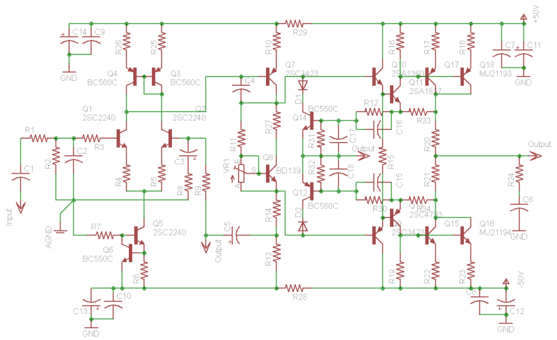
EDIT: Oops... R12,30 should be connected directly to R20,21 not the drivers.
I haven't given up on the dual driver version; I'll probably prototype, or atleast simulate both versions. Good point on transistor Ft. What devices were used in that amp you mentioned, sakis?
So, Q8 will mount in contact with the drivers, as in a regular CFP output stage, and the pre-drivers don't need to be included.
Here is where we are now, with the single driver version. I've now got all the features included that I wanted originally. The diagram is getting more complicated; let me know if I need to move something around to make it legible. I see now why when amps start getting past simple circuits people drop the component values, and make a separate parts list. 🙄
EDIT: Oops... R12,30 should be connected directly to R20,21 not the drivers.
Last edited:
Getting there...
You nearly have a workable amp.
You have D2 inverted (on the current limit), change round to make it work 😉 Also i'd alter the position of the current sense connections to the collectors of the output pairs. No point in sensing it at the emitters of the drivers...
Other than that it should work.
The only other thing i'd do that will improve the performance is to add another resistor in series with R7 to ground (constant current on the input stage LTP) & at the juction between the new resistor & R7 connect the positive end of a 10 or 22UF electrolytic & then connect the negative end to the - rail. This will increase the PSRR (power supply rejection ratio) of the constant current & lower the noise floor of the amp 🙂
You nearly have a workable amp.
You have D2 inverted (on the current limit), change round to make it work 😉
Good catch, thanks.
Also i'd alter the position of the current sense connections to the collectors of the output pairs. No point in sensing it at the emitters of the drivers...
I noticed that after I posted the schematic...
The only other thing i'd do that will improve the performance is to add another resistor in series with R7 to ground (constant current on the input stage LTP) & at the juction between the new resistor & R7 connect the positive end of a 10 or 22UF electrolytic & then connect the negative end to the - rail. This will increase the PSRR (power supply rejection ratio) of the constant current & lower the noise floor of the amp 🙂
I'll make these corrections/improvements and repost the schematic. Rough idea to semi-final design in less than 48hrs... Not bad! Thanks for the help everyone.
Here it is. Protection circuit is a complete rip from the Low TIM Leach. I think everything is good now; I still need to figure out how to calculate C3 and C5 Fc points, though... And simulate, prototype, build, etc...
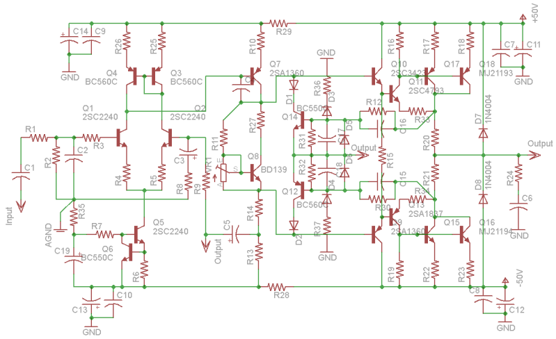
Also, I forgot to add the current limiter to Q7. Kind of defeats the purpose of a protection circuit if the VAS blows up anyway.
C3 which is the DC blocking capacitor on the base of the transistor in the LTP will give you the low frequency cutoff of the amplifier (you'll find that C1 & R2 will have the same effect). A lot will depend on the value of the feedback resistor from the output, the lower value you make that feedback resistor the higher the value of the capacitor will need to be for a certain f3.
There are certain advantages to using a lower value resistor in the feedback loop, you can reduce the amplifier noise floor. However to keep the offset voltage low you'll want a similar value of resistor from the base of the amp input transistor to ground. This may result in a quite low input impedance, though there are ways round this, something for the future possibly 🙂
Keep it up, a bit of current limiting on the Vas transistor & you are ready to simulate.
By the way, C5 make about 100pf or higher to start with & you should have a stable amp. It can always be reduced if you test the amp & it proves to be over compensated. Better safe than sorry...
So, Fc of C3 is calculated using 1/2pi(R9)(C3). C5 is the bootstrap capacitor, 100pF would be a bit small there. 😀 C4 is the miller comp cap; 100pF would be appropriate there. I think C5 would also be based on the value of R9, the feedback resistor, if I'm looking at it correctly.
Its starting to look like a complicated mess now.
So many capacitors ! It has loads of transistors for gain then the gain is removed by capacitors so might as well just use less transistors.
It hasnt even got a CCS for bias which might cause problems.
So many capacitors ! It has loads of transistors for gain then the gain is removed by capacitors so might as well just use less transistors.
It hasnt even got a CCS for bias which might cause problems.
Its starting to look like a complicated mess now.
Thank you for your constructive opinion.
So many capacitors ! It has loads of transistors for gain then the gain is removed by capacitors so might as well just use less transistors.
It hasnt even got a CCS for bias which might cause problems.
I'm not sure what caps you mean, or how you think they remove gain. You're going to have to be more specific if you want to contribute positively to this thread.
The main thing that makes this design more complicated than a typical DIY design, is the protection circuit. In my opinion, regardless of how many DIY amps lack current limiting, it is very necessary for a professional, reliable amplifier. This amp is still less complicated than a Leach, and many others, and should still have similar performance once I'm done.
I chose not to use a CCS in the VAS, and probably won't unless it shows significant improvement to the design in simulation.
- Status
- Not open for further replies.
- Home
- Amplifiers
- Solid State
- A "Patchwork" Type Concept Amp