This is the kind of stupidity that emerges when you edit your own text without proofreading carefully. lolI wanted the GND to first be filtered out by the capacitor, then by the decoupling capacitor before reaching D901 of the DC Servo.
To explain further, I edited three times my comment above before this last version. Having my weird trace in mind, I wrote that "I wanted to filter the +/-15 VDC rails". But once observing my PCB traces, I realized that the weird trace wast the +/-15 VDC traces but the ground trace! You know the rest lol...
So...
To resume :
More to come in a near future...
To resume :
- Different ground traces for each sections, reaching the PCB HQG
- Center the PCB HQG
More to come in a near future...
the "star" grounding method has been mention several times, but trying to star to one point can get messy, see post 13, all those links.
do not overlook the "buss" grounding method, which gives a structured approach, and a combination of both buss and star.
do not overlook the "buss" grounding method, which gives a structured approach, and a combination of both buss and star.
Having the output transistors in the same vertical line does not help in optimum utilization of the heat sink area! See if they can be staggered.
Agreed!Having the output transistors in the same vertical line does not help in optimum utilization of the heat sink area! See if they can be staggered.
When I waked up this morning, I realized that all my arguments to stay with my approach are based on the fact that I still keep my first project mechanical limitation; the holes positions standard in the heat-sink, offered by Modushop.
But nothing force me to stick with these. In reality, I started my first project with them in the hope that in case if anyone could be interested to acquire my final PCB, they would have been compatible with their own Modushop heat-sink.
Also, my first frontier is always the big can that must be between two holes in a row. And this issue force me to keep them close to the PCB border, as close as I can with their respective transistors. And at some points I cannot respect that with the Power resistors present in the rail path.
So in my next iteration, I will erase all those holes from my path and will instead try to place them at each corner of the PCB.
The worse result will be that I will have to make new mounting holes in the heat-sink.
I have this question related to the ground path of my IPS.
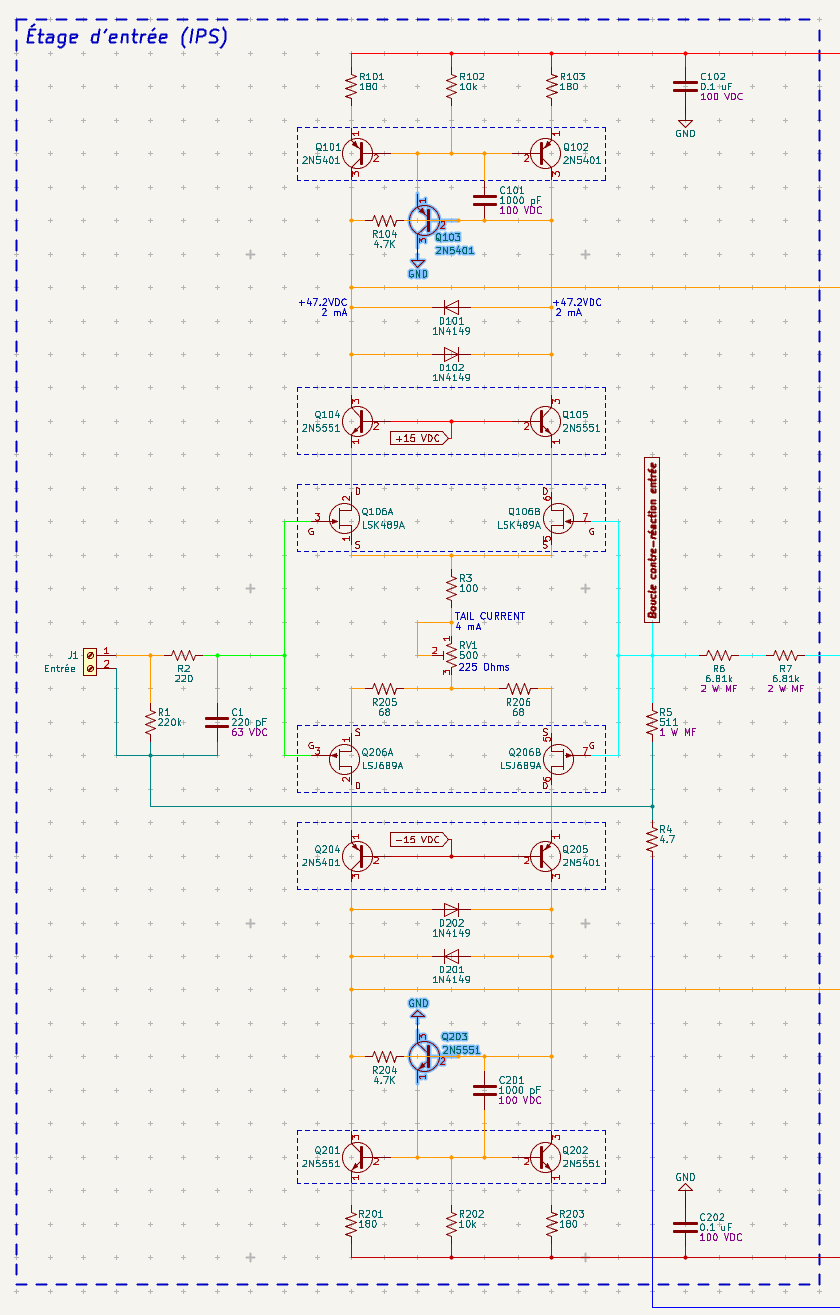
From preceding commentary's, I understood that the Input ground traces from the junction of R4 and R5 to the Input connector and parts J1 pin 2, R1 and C1, must be as close and as short as possible, with nothing else connected to them. Others commentary's said that the decoupling capacitors C102 and C202 ground return should never connect to the IPS ground, but instead to the HQG, so to make sure that no residual noise can be injected into the IPS ground. But what about the IPS ground traces from collectors of Q103 and Q203 (highlighted) ?
Do they have to be connected to the HQG with their own traces or they are part of the IPS section and can be connected to the IPS ground of connector J1? What about connecting them to the C102 and C202 ground traces?
This is bugging me!
You want the ground on Q103 & Q203 to be as quiet as possible, so they should connect to the input ground IMO. Don't connect to C102 and C202, that's the power supply ground and is liable to be noisy.
Thanks kapitiaudio. That was my though also. But my doubt about this solution is that nothing should be connected to the Input, to minimize the injected noise at the input. The third solution would be to connect them to the VAS ground audio part.
But I am now facing another reality. I really ask myself if the layout of the complexity of the Figure 14.17 topology is feasible into a PCB limited by a 3U heat-sink height!
Since my last post, I am at my fourth PCB layout iteration, without success! The "bridge to cross" is always the final connections that must travel the length of this physical board. My latest iteration, still with traces not completed, could be finalized and maybe contour this issue if I moved the protection diodes of the OPS in the center of the board. This actual configuration is the only one that meets all electrical requirements:
Honestly, does someone has achieved a complex topology as this one into a 3U heat-sink? I mean with the final board screwed on the heat-sink?
For your eyes only, here some captures of the fourth latest iterations, with their problem commented...
Original design built-ed into the AMP. Ground loop problem with the folding rail traces:
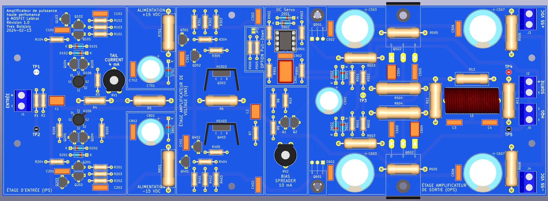
Iteration 1. FB ground loop trace to long:
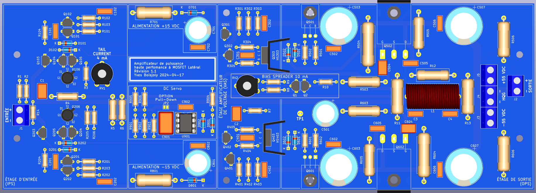
Iteration 2. FB ground loop minimised, but still to long:
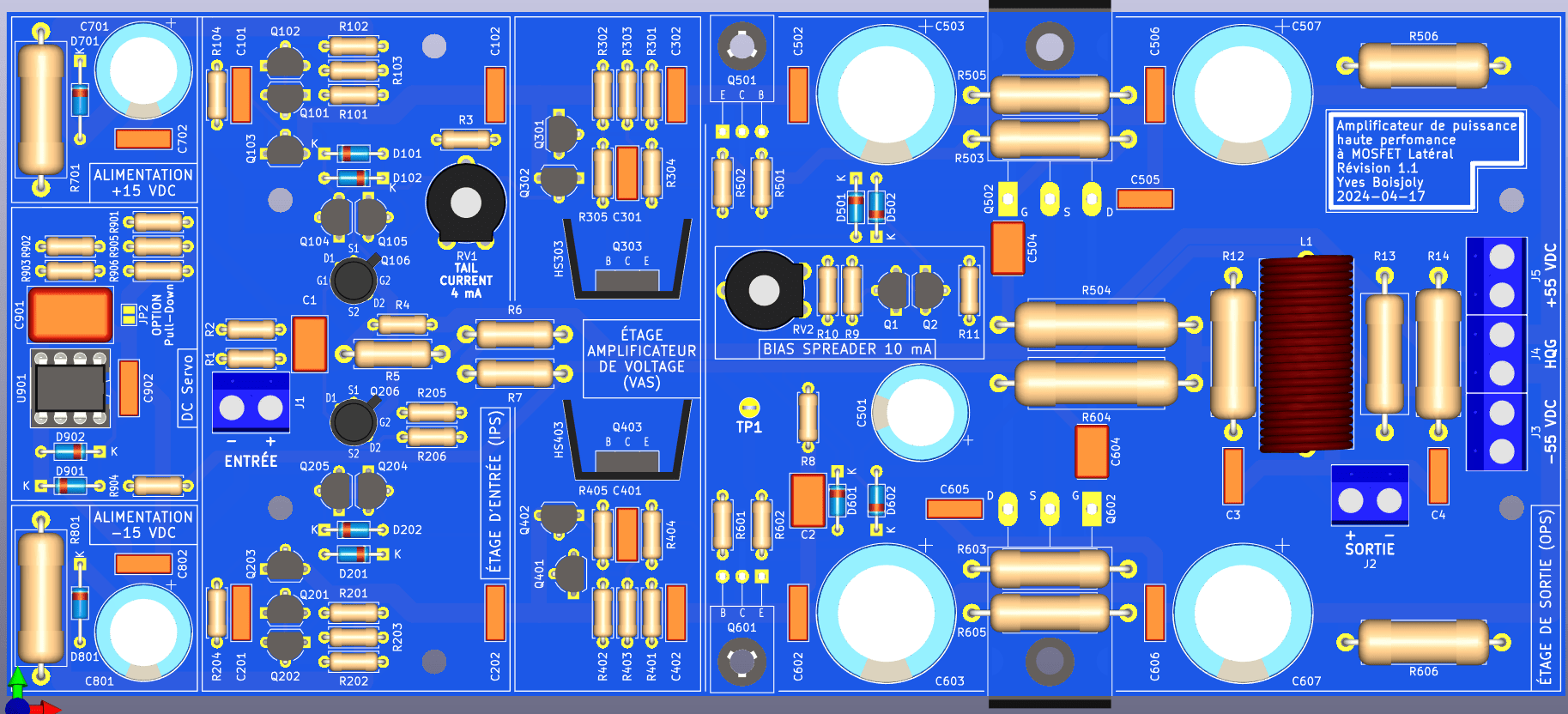
Iteration 3. Abandonned beause the final traces couldn't be completed:
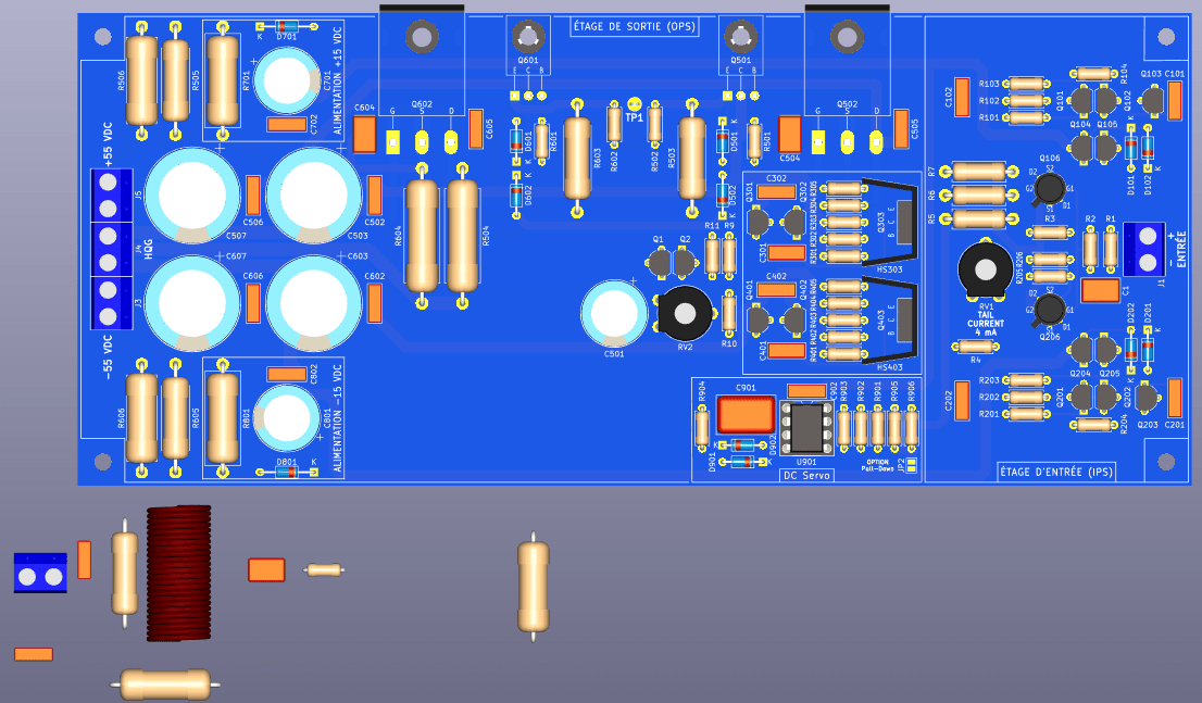
Iteration four. In this layout, I though "Why can I simply put the MOSFET at the end of the PCB instead of trying to keep them fixed on the pre-fabricated 3U holes at the top". And once near the end of the final layout, it came back to my mind that the MOSFETs should be as close as possible one to each other! Although, this layout has the shorter FB traces possible, with it's FB resistors between the Input and Output connectors! And I admit I like the simetrical IPS and VAS layout, with the screw space optimised by the little TO-220 heat-sinks position!
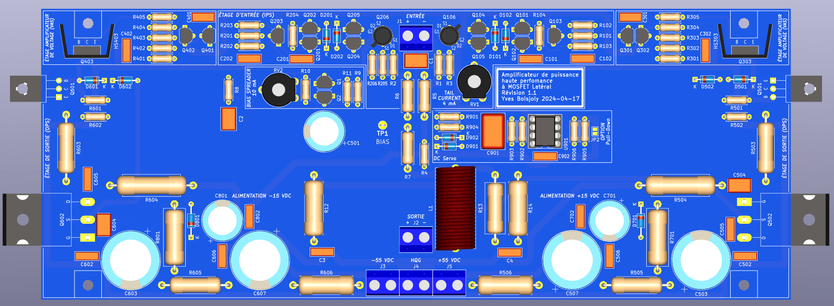
But I am now facing another reality. I really ask myself if the layout of the complexity of the Figure 14.17 topology is feasible into a PCB limited by a 3U heat-sink height!
Since my last post, I am at my fourth PCB layout iteration, without success! The "bridge to cross" is always the final connections that must travel the length of this physical board. My latest iteration, still with traces not completed, could be finalized and maybe contour this issue if I moved the protection diodes of the OPS in the center of the board. This actual configuration is the only one that meets all electrical requirements:
- Shorter FB traces
- Shorter RAIL traces with their ground traces under them. Although they are still in a folding design, they are much much short than all my previous ones.
- Shorter Input ground traces
Honestly, does someone has achieved a complex topology as this one into a 3U heat-sink? I mean with the final board screwed on the heat-sink?
For your eyes only, here some captures of the fourth latest iterations, with their problem commented...
Original design built-ed into the AMP. Ground loop problem with the folding rail traces:
Iteration 1. FB ground loop trace to long:
Iteration 2. FB ground loop minimised, but still to long:
Iteration 3. Abandonned beause the final traces couldn't be completed:
Iteration four. In this layout, I though "Why can I simply put the MOSFET at the end of the PCB instead of trying to keep them fixed on the pre-fabricated 3U holes at the top". And once near the end of the final layout, it came back to my mind that the MOSFETs should be as close as possible one to each other! Although, this layout has the shorter FB traces possible, with it's FB resistors between the Input and Output connectors! And I admit I like the simetrical IPS and VAS layout, with the screw space optimised by the little TO-220 heat-sinks position!
I just got this "brilliant" idea...
Turning the board 180 degrees on itself, to liberate the pre-drilled holes in the heat sink for the Output MOSFETs!
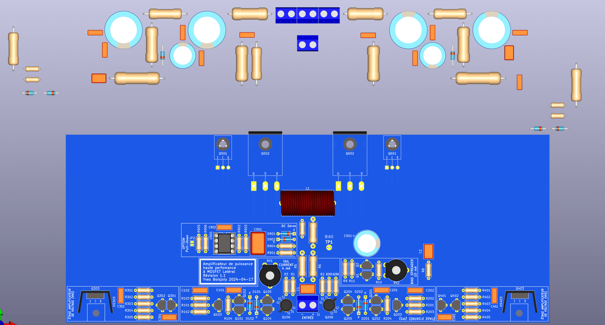
Turning the board 180 degrees on itself, to liberate the pre-drilled holes in the heat sink for the Output MOSFETs!
I have finished the fifth iteration and this time I really think I achieved the best PCB design possible.
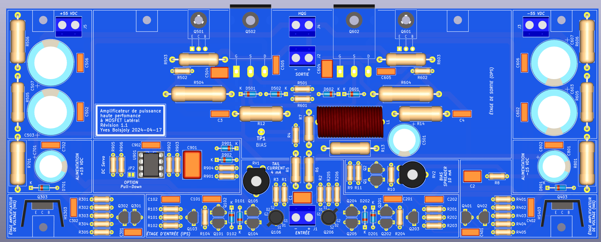

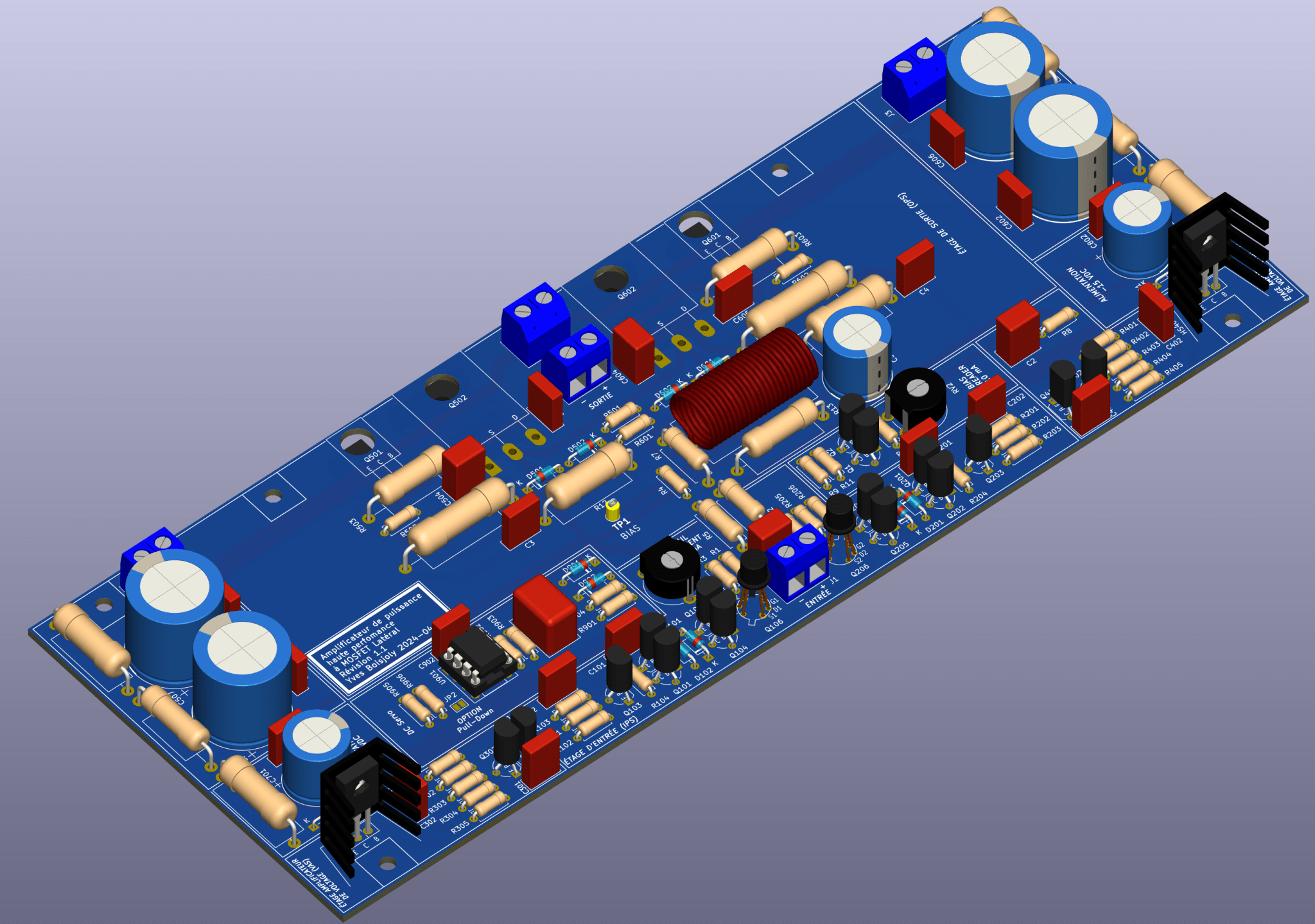
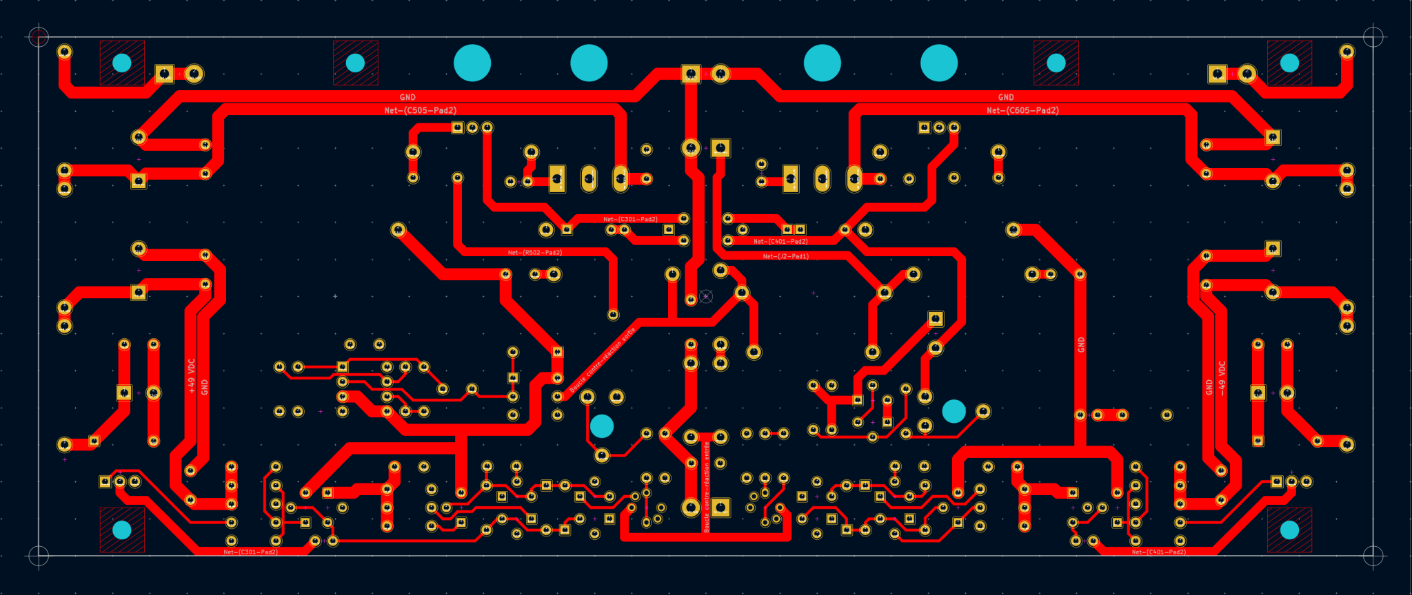
Ground traces. Some of the Red traces are invisible under the Blue traces along the top of the PCB. See the individual sides captures below:
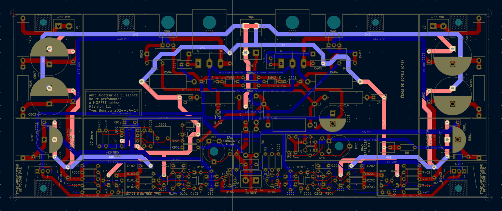
FB loop traces:
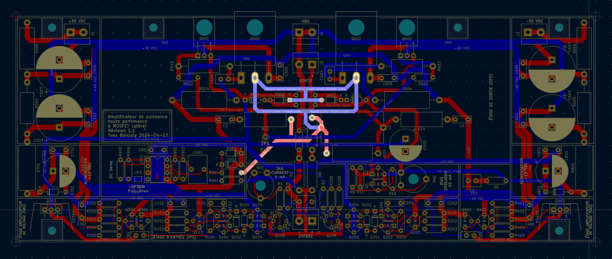
Components side:
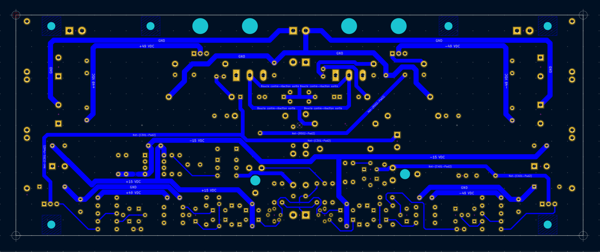
Solder side:
Mechanical on the Heat-Sink. The board is now shorter than the previous design and the leftmost and rightmost holes aren't used anymore:
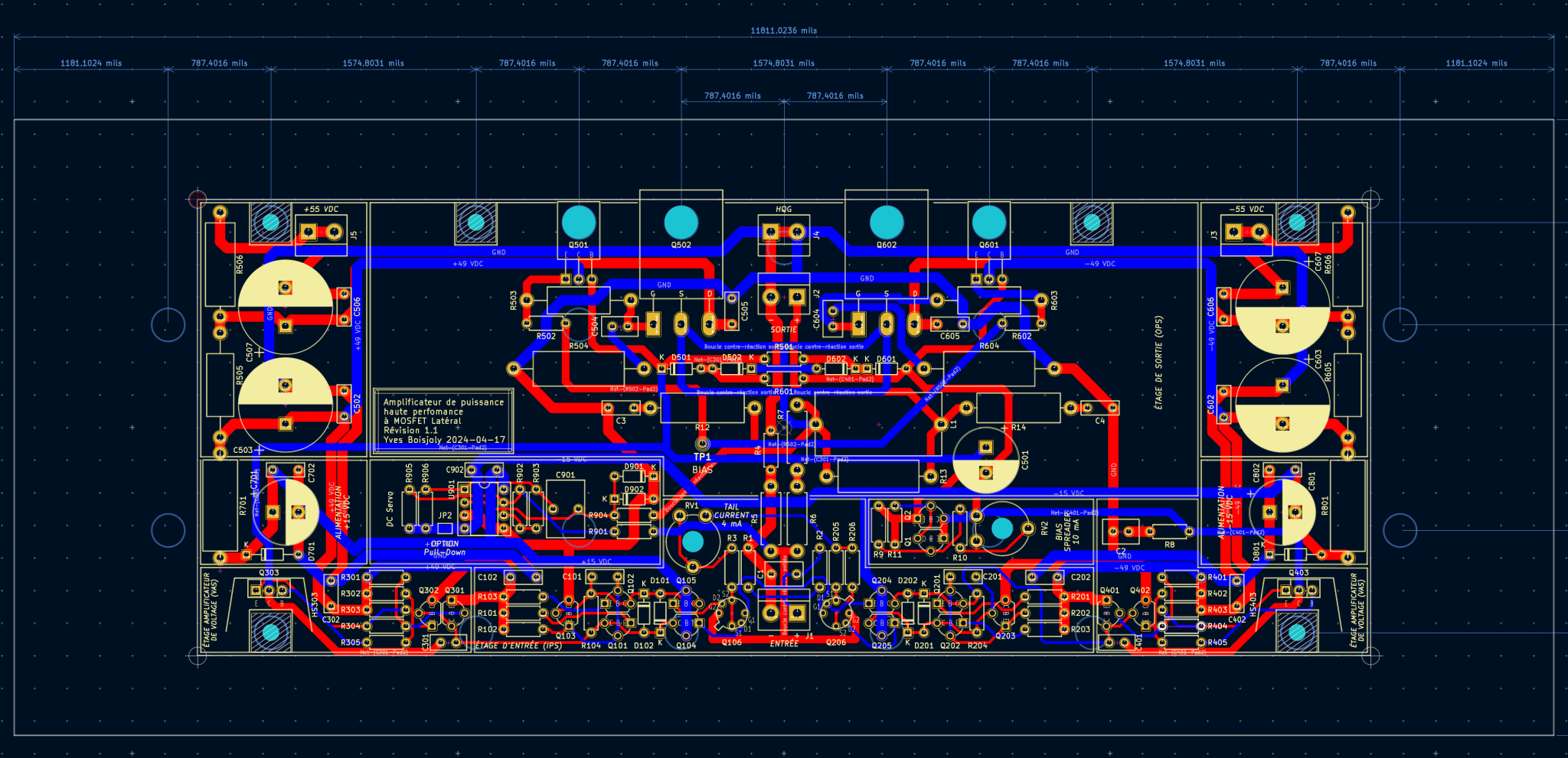
- Output transistors are placed close together and distributed along the heat-sink to optimize heat dissipation.
- Feedback loop paths are kept as short as possible.
- Input and output connectors are close and centered, so that inversion of the printed circuit boards in the case will not influence the path of their respective wires. Only the power supply rails will be opposite. The input connectors will be located towards the top of the box to allow the wires to run along the cover to the RCA connectors on the rear panel. The Output, Power and HQG ground connectors will be near the perforated panel at the bottom of the case.
- I've optimized the space required by the heat sinks for the VAS Q303 and Q403 transistors by positioning them close to the PCB mounting screws.
- All power supply rails are close to the ground rails to minimize noise injection.
- The ground rails are all independent and join the star-shaped HQG ground.
- The DC Servo circuit is close to the feedback loop, and its input/output traces are kept to a minimum.
- Much to my surprise, I had no trouble getting past the various traces, and plenty of free space remained available.
Ground traces. Some of the Red traces are invisible under the Blue traces along the top of the PCB. See the individual sides captures below:
FB loop traces:
Components side:
Solder side:
Mechanical on the Heat-Sink. The board is now shorter than the previous design and the leftmost and rightmost holes aren't used anymore:
Thanks!I think this approach is much better!! Beautiful board.
But I just had this new idea. Wouldn't be much better if I move the four Power transistors of the OPS one hole to the left and one hole to the right. And move the two mounting screws in the center, close to the HQG connector? I just realized that there are no traces in the path. That would distribute the heat much better, but I wonder if the traces that join the two MOSFETs would suffer from this extra length created...
Good idea.
Also, since you have some empty spaces on upper left/right side of the output transistors, you could move big capacitors in there, and make whole board more narrow?
Also, since you have some empty spaces on upper left/right side of the output transistors, you could move big capacitors in there, and make whole board more narrow?
Its looking pretty good, although I have some observations.
You have two long loops to left and right carrying non-linear half-cycle currents, I think it would be better to place the capacitors close to the output devices to minimize loop area, say on the board underside. And thicker traces for the high current paths unless they its a 2oz PCB. I would route the +55V/0V/-55V on one cable with 3-pin connector to the amp, again minimizing loop area for non-linear current paths.
In several amp designs I've separated the output stage to a separate PCB even, which helps keep input signal circuitry further from the high current parts, and allows less-fraught commissioning and fault-finding as each PCB can be investigated separately.
Yves, Here is an example of a PCB from Nmos Quasi Amp from this thread.
It's much simpler amp, but the PCB shows nicely the idea of centralized star-shaped grounding.
I think this kind of grounding would work much better, and that's what I'm using in my PCBs.
View attachment 1304848
Great design. I like it!!
A minor change that should reduce distortion... especially at high listening levels (high current draws speakers <-> output MOSFETs):
Another idea. If you're able to make the PCB taller, then you can put the power supply directly behind the output transistors to shorten the traces and reduce loop area. Also, there's not enough clearance between your GND and B+/- rails (+/-49V). A bit of dirt or contamination could cause a conductive path to develop which if left long enough can eventually cause the PCB to catch fire lol.
Yes all my boards are 2 oz copper. I think you missed the overall history of this PCB. This board is intended to be mounted on a 3U heat-sink from Modushop! There is no place under the board to place the capacitors.And thicker traces for the high current paths unless they its a 2oz PCB
Again 2oz copper.high current draws speakers <-> output MOSFETs)
Same comment as Mark Tillotson above. Read the history please!Another idea. If you're able to make the PCB taller, then you can put the power supply directly behind the output transistors to shorten the traces and reduce loop area. Also, there's not enough clearance between your GND and B+/- rails (+/-49V). A bit of dirt or contamination could cause a conductive path to develop which if left long enough can eventually cause the PCB to catch fire lol.
Some comment says to run the rail traces as close as possible to the ground traces to minimize noise injection. This board will have a solder and components mask that should keep away contamination.
Here is the fifth design updated with Minel123 comments above. I replaced the footprint of R3 and R10 from 0.3" to 0.4", in the goal to have tests points to calibrate the 4mA TAIL Current (400mV / R3_100 Ohms = 4mA) and 10mA BIAS SPREADER (3.3V / R10_330 Ohms = 10mA)
Ground:
FB Loop:
Components side:
Solder side:
Overall:
I did read the history. Mark commented on trace thickness. I'm commenting on trace clearances. Your new design is still has the same issue, the B+/- rails don't have enough clearance to ground. A solder mask is not a reliable insulator.
@kapitiaudio
What would be your suggestions for a minimal traces width for a +/-50 VDC rails, 2oz copper? And what would you recommend for the minimal space width between them?
Thanks in advance.
Regards
What would be your suggestions for a minimal traces width for a +/-50 VDC rails, 2oz copper? And what would you recommend for the minimal space width between them?
Thanks in advance.
Regards
- Home
- Amplifiers
- Solid State
- A Lateral MOSFET Power Amplifier Design Version 1.1