Hello,
Following Bonsai constructive comments and advises,
Ref.:
with the HBR resistor added, and a totally new traces strategy.
I'd like to share the schematics and the new PCB captures for your comments. I am very open to any comments or advises from every ones...
My bests regards and, thanks in advance...
P.S.: Schematic attached below in PDF format.
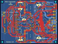
01-Ground Components Side highlighted

02-Ground Solder Side highlighted

03-Rails Traces over respective grounds (grounds highlighted)

04-Ground Loop Area

05-Silkscreen on top

06-Silkscreen and Ground Loop Area

07-3D View-Top

08-3D View- Iso

Following Bonsai constructive comments and advises,
Ref.:
- https://www.diyaudio.com/community/...as-a-small-sizzling-sound.411503/post-7659500
- https://www.diyaudio.com/community/...as-a-small-sizzling-sound.411503/post-7660158
with the HBR resistor added, and a totally new traces strategy.
- I removed all tests points except TP3, now renamed TP1
- I moved the DC Servo closer to the IPS.
- I made Rails connectors closer to each other.
- The BIAS Spreader is closer to the VAS
- I minimized the ground loop area at the IPS
- I passed the +Rails and -Rails in folder view with their respective own ground traces under them, on the other side of the PCB
- I kept the Signal ground return track close to the feedback track to minimize the possible ground loop, I also kept it without nothing connected to it.
- I added the 4.7 Ohms HBR resistor, close to the input.
- I put the speaker output at the very end of the traces.
I'd like to share the schematics and the new PCB captures for your comments. I am very open to any comments or advises from every ones...
My bests regards and, thanks in advance...
P.S.: Schematic attached below in PDF format.
01-Ground Components Side highlighted
02-Ground Solder Side highlighted
03-Rails Traces over respective grounds (grounds highlighted)
04-Ground Loop Area
05-Silkscreen on top
06-Silkscreen and Ground Loop Area
07-3D View-Top
08-3D View- Iso
Attachments
Looks good! I have a couple of suggestions. What happens when R506/R606 get hot? Could it melt the plastic on the electrolytics? Perhaps a bit more spacing would be prudent? Also, its seems the the small 2-terminal input screw connector is obstructing the larger one, making wires difficult to insert.
R506/R606 Good point! I moved them away...What happens when R506/R606 get hot? Could it melt the plastic on the electrolytics? Perhaps a bit more spacing would be prudent? Also, its seems the the small 2-terminal input screw connector is obstructing the larger one, making wires difficult to insert.
the small 2-terminal input screw connector is obstructing the larger one
Agreed. It was center and I noticed that. So I move it above at middle of the two Power one. Seeing each bloc have two screw, once moved you can connect the wires on the top one of the +rail and on the bottom one of the ground. But I will have a look to see if I can do better...
I have predefined class of traces wide. All the signals traces have 0.010 inch. It is more than needed. But I could may be make them wider when space is available. Well noted.Why so thrifty with the thickness of the tracks ? Dont know if i am wrong, but i try to make the tracks as thick as the pads / vias.
Good morning,
Following the above suggestions :
Don't hesitate again to share your opinions...
Regard and thanks in advance

Following the above suggestions :
- I replaced all ground traces from 70mil to 80mil
- I replaced all rails traces from 60mil to 80mil
- I replaced all other traces from 10mil to 20mil
- I moved the two Upper FB resistors R5 and R6 to the right to minimize the effect of their rising temperature on the IPS transistors
Don't hesitate again to share your opinions...
Regard and thanks in advance
Sevy, I just have one general observation about this board - because you chose to design it so it corresponds exactly to the schematic - reading from left to the right side, with consecutive blocks (input/opamp/vas/output) - all the traces look too long to me.
Especially these long +/- supplies, ground and feedback traces spanning across whole board.
It looks nice, and is 'readable' - easy to match it with the schematic, but the consequence is long traces.
So the bottom line - pcb looks too big, with traces being too long. I'm sure it can be designed as smaller one, with shorter traces.
Not sure if I'm right, it's just an opinion/feeling.
Thanks for your comments minek123! They didn't fall on deaf ears.So the bottom line - pcb looks too big, with traces being too long. I'm sure it can be designed as smaller one, with shorter traces.
We still need to keep in mind that my design are based on the 3U Heat-sink, that is limited in height versus it's wide width.
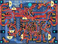
So I had redo all the board, this time using 0.300" pins spacing for all 1/4W resistors, instead of the preceding design that had 0.400" pins spacing. I also used my first board strategy to put big resistors on top of the MOSFETs, seeing that they are on the other side, under the board.
With that, I achieved a reduction of 2.025 inches. The old version was 10 inches wide, this one is only 7.975 inches wide. I hope this will put the input connector a bit more away from the transformer. I also placed the FB resistors along the path to minimize the trace length of the feedback return. And I accepted the unaesthetic placing of the input and output connectors to have them close to the back panel.
I kept the folder version of the rails, with their respective ground traces under them on the solder side.
Again, I share some captures for every one interested. It is never finished, so commentaries are again welcome ;-)
Top traces with silkscreen:
Bottom traces with silkscreen:
Both traces and silkscreen, for overview of rails and grounds:
Feed-back Loop in Yellow:
3D plan and isometric views:
I'm not sure why the DC servo is taking its input at the far side of the output inductor coil, and in order to do that you ended up running a separate trace all the way from the output to the front end. Most (if not all) amps that I saw having a DC servo get input at the near side of the output coil, and that they do not need that separate trace.
If taking the far side of the coil is necessary, considering that node hooks up with the outside-going cable directly, therefore may subject to RF ingression, I would put a resistor, 1k-ohm or so, in series with the trace, close to the coil, so as to confine the extension of the speaker cable from going deep into the layout, and to the front end.
If taking the far side of the coil is necessary, considering that node hooks up with the outside-going cable directly, therefore may subject to RF ingression, I would put a resistor, 1k-ohm or so, in series with the trace, close to the coil, so as to confine the extension of the speaker cable from going deep into the layout, and to the front end.
Looks much better now. The smaller the better.
Just a philosphical") observation:
observation:
I think all the grounds traces will be shorter and easier to route, if ground PCB connector was for example in the centre of the PCB.
No one ever made it a law, that all connectors (including rails) have to be on the edge of the board.
Also, sometimes, if I'm size contrained, I tend to place some small resistors or caps or diodes on the bottom side of board, to save space, or simplify the traces.
Just a philosphical
observation:I think all the grounds traces will be shorter and easier to route, if ground PCB connector was for example in the centre of the PCB.
No one ever made it a law, that all connectors (including rails) have to be on the edge of the board.
Also, sometimes, if I'm size contrained, I tend to place some small resistors or caps or diodes on the bottom side of board, to save space, or simplify the traces.
Last edited:
Hum... To be honest, after having read your comment, I searched in all my books where I could have pick up this rule. I never find anything arguing that it should be at the far edge of the coil, except that most reading said that the DC servo should take it's input at the Amplifier Output.I'm not sure why the DC servo is taking its input at the far side of the output inductor coil, and in order to do that you ended up running a separate trace all the way from the output to the front end. Most (if not all) amps that I saw having a DC servo get input at the near side of the output coil, and that they do not need that separate trace.
If taking the far side of the coil is necessary, considering that node hooks up with the outside-going cable directly, therefore may subject to RF ingression, I would put a resistor, 1k-ohm or so, in series with the trace, close to the coil, so as to confine the extension of the speaker cable from going deep into the layout, and to the front end.
The weird thing is that I remember having consult once a diagram that make me connect it that way, but I never found it back from all my reading :-/ And from all the books I have (Bob Cordell, G. Randy Slone, Douglas Self), there are no schematic that show where the DC Servo Input is taken from. Only a schematic of the DC Servo itself, out of the whole schematic.
So I guess it would be much better be connect the DC Servo Input at the far left side possible of the board, just at the R7 pin of the FB.
From there:
To there:
Like this, highlighted:
No, but I received comments in the others threads that the +VCC traces should be as close as possible to it's ground trace or on top of it on the other side of the PCB, idem for the -VCC. Keeping in mind that I always have made my design respecting the holes positions of the 4U heat-sink that is available from Modushop, but applied to a 3U heat-sink, and that my holes are already made on each heat-sink. I have to keep already mounting holes made available and this, with the resistors R505/506 and R605/606 in the rail paths crossing their owns decoupling capacitors and cans, make it much easier to start from one point and follow a straight lines over every sections sequentially, like this; OPS -> VAS -> IPS -> +/-15VDC Zener and components -> and finally Q104/105 and Q204/205 +/-15VDC requirements).No one ever made it a law, that all connectors (including rails) have to be on the edge of the board.
See the mounting holes available below:
Yves, Here is an example of a PCB from Nmos Quasi Amp from this thread.
It's much simpler amp, but the PCB shows nicely the idea of centralized star-shaped grounding.
I think this kind of grounding would work much better, and that's what I'm using in my PCBs.

It's much simpler amp, but the PCB shows nicely the idea of centralized star-shaped grounding.
I think this kind of grounding would work much better, and that's what I'm using in my PCBs.
That layout does pose a visual candy. But there is room for improvement. 1/ The feedback-return loop could be more tightened up. @Sevy layout has a much smaller loop area despite much greater dimension PCB. 2/ the feedback takeoff point screams at me in the face, perfect example how not to do it.Here is an example of a PCB from Nmos Quasi Amp from this thread.
@nattawa I am not sure to well understand your reference for this second observation. You quoted minek123 sentence but address your comment to me. Do you mean that my PCB has a bad takeoff point or instead that this PCB example has a bad takeoff point?2/ the feedback takeoff point screams at me in the face, perfect example how not to do it.
And @minek123, when I compare the schematic from your link versus the PCB picture above, all references are not onto the PCB except the transistors, so it is hard to follow. Secondly, I am not saying that your suggestion about the ground input is a bad choice, but comparing the complexity of this design versus mine, the latter is much more complex with Power resistor in series between Power Supply and the OPS, as well as from the OPS and the VAS, each with their own big caps and decoupling caps. In my design. I force every traces to respectively reach the big capacitor first, then the decoupling capacitor, and then the trace reach it's respective section parts. That explain the weird traces coming out from the Zener diodes GND rails. I wanted the GND to first be filtered out by the capacitor, then by the decoupling capacitor before reaching D901 of the DC Servo.
Last edited:
Both points in my comment were about the example minek123 posted. Your design was mentioned in my comment to show how that example could be improved. It meant to read "@Sevy's layout". Perhaps the spell check did not like it that way.@nattawa I am not sure to well understand your reference for this second observation. You quoted minek123 sentence but address your comment to me. Do you mean that my PCB has a bad takeoff point or instead that this PCB example has a bad takeoff point?
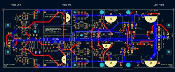
I have made a screenshot of one older version of your pcb. I have marked "Fields"
In the first and second field you can get the pcb much smaller. The DC servo can remain in the second field, nearer to the output and not to far from the input. You have only to arrange the components in an other way. You give away space...
In the last field you can choose the resistance R506/R606 parallel to the capacitors and you have an new arrangement to output and railvoltage in one line.
I think you choose metz connectors or similar...
Another question...have you ever decided to use a groundlane on your pcb ? There a different oppinions about groundplanes, i know. I always got good experiances with a groundplane. Destroyer X gave the advice not to use a groundplane on its Blame ST's.... i can say...it works with a groundplane. No hiss no hum. You can see the pcb on the second picture...
Perhaps there is a reason not to use a groundplane in your amp..dont know...
Peter
Attachments
I gave the example of the Quasi Nmos PCB to show the star-shaped grounding of the amp.
All responses focused primarily on some other aspects of the PCB.
GND "filtered" ? That must be some new concept.
Whenever we are dealing with big electrolytic caps, we are also dealing with big, pulsating currents (under load).
These currents are flowing from the caps to both: ground and rail connection.
It is not good idea to feed the SAME ground trace to any previous stage of the amp. These traces should be feeding output stage only.
Previous stages should connect ground back to the main GND point of the PCB. They might have their own electrolytic cap(s) if needed.
It should not be a "chain" of one solid GND path feeding each stage of the amp, and accumulating on its way all kind of pulsations of currents.
And this is easier to achieve, if GND connector is placed in the middle of the PCB.
That's what Quasi's PCB was supposed to illustrate.
All responses focused primarily on some other aspects of the PCB.
I wanted the GND to first be filtered out by the capacitor, then by the decoupling capacitor before reaching D901 of the DC Servo.
GND "filtered" ? That must be some new concept.
Whenever we are dealing with big electrolytic caps, we are also dealing with big, pulsating currents (under load).
These currents are flowing from the caps to both: ground and rail connection.
It is not good idea to feed the SAME ground trace to any previous stage of the amp. These traces should be feeding output stage only.
Previous stages should connect ground back to the main GND point of the PCB. They might have their own electrolytic cap(s) if needed.
It should not be a "chain" of one solid GND path feeding each stage of the amp, and accumulating on its way all kind of pulsations of currents.
And this is easier to achieve, if GND connector is placed in the middle of the PCB.
That's what Quasi's PCB was supposed to illustrate.
Last edited:
Here is another example, with the same concept taken even further: this PCB has 2 GND connectors.
1) "Dirty GND" for the output stages
2) "Clean GND" for the input stages
Each of them has separate wires to the central GND point at the PSU.
This way we don't need "lifted ground" cheat/trick with a resistor for the input stage GND, and we can still avoid hum.
Each of these GND connectors on the PCB is more or less central, to avoid long GND paths.
This PCB (from this thread) is only 4cm x 8cm, and also shows correct point of taking the feedback path from the output.
The feedback trace is only 2.5cm.
I know this is much smaller amp (hence smaller PCB), but it's used as an illustration of a concept.
Similar, centralized design with 2 GND connectors can be seen in Bonsai's KX amp in this post:
https://www.diyaudio.com/community/threads/hifisonix-kx-amplifier.329814/post-6434250
- Home
- Amplifiers
- Solid State
- A Lateral MOSFET Power Amplifier Design Version 1.1