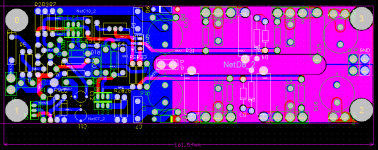
As far as I have undestood I need to make a clean star ground and the center of star ground connect by wire with dirty ground at power supply.
I have made semi-star ground. Connected input filter ground together and routed common wire to star.
Now ground routing ok?
I have made semi-star ground. Connected input filter ground together and routed common wire to star.
Now ground routing ok?
Attachments

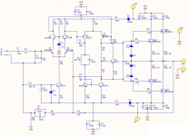
hi guys, i have done the same amplifier, but i have some problems.
the schema is show below.
the transistors q6 q7 q8 q9 e q5 are quiet hot, but the real problem is that i haven't no voltage across the source's resistors.
the voltages across R2 R3 R7 R25 R29 are slightly lower of the voltages writes on the pre-flight test in the holton's document, i think that's is normal..
i have done all pre-flight test with a 10ohm resistor across d4-d8 (in the schema below), but at the final test i saw that i have no voltage across the sourse's resistors.
please someone could help me??
sorry for my english!!!
Thanks
Attachments
hi, thanks for your interest in my problem..
i hve misurated some voltages across some components
in first:
R7 0.911V
R9 14V
R17 25.4V
C5 6.02V
and:
R2 1.43V
R6 40.8V
R3 1.45V
R25 0.440V
R29 0.478V
R14 43.8V
and across Collector and Emmitter of these transistors
Q3 37.2V
Q4 39.6V
Q1 14.9V
Q2 14.9V
Q5 14.7V
Q8 65.1V
Q9 51.3V
Q6 0.585V
Q8 51.6V
Q10 5.6V
across D4-D8 3.03V
across D4-D8 2.99V
i rotate the pot, P1, but i haven't see variation across source resistors
have any idea of the mistakes??
thanks a lot
Hi,
check r25 & r29 again.
check the voltage around the Vbe multiplier.
The current through Q10 + R14 adds up to more than the current through R29. Note also the unbalance between R25 & R29. are the MJEs matched?
Something odd happening here.
Vgs~=3V, seems OK for a vFET. Where is the source current? Maybe your FETs need ~4Vgs to start conducting. Have you connected the Vfets correctly. The pin out is different from an Lfet.
try Vbe multiplier down at minimum voltage.
Now add a 20k in parallel to R9, thus increasing the LTP tail current from 1.4mA to 2mA. check the voltages across the LTP and VAS emitter resistors.
Do all this with power off and only power up through a mains light bulb until you know the circuit is working properly.
Have you fitted fuses in the power rails? Have you replaced these fuses with ~400mW 100r temporary resistors?
i have find a serius problem.. my mosfet are fake!!!
i bought them at the electronic fair 2 month ago, and i haven't test them first!!
now i have ordered new mosfets at 2,50€ each, and i attend to these..
thanks a lot for your time and your help.. i'll write for some news as soon as possible
thank's a lot
bye
🙂
i bought them at the electronic fair 2 month ago, and i haven't test them first!!
now i have ordered new mosfets at 2,50€ each, and i attend to these..
thanks a lot for your time and your help.. i'll write for some news as soon as possible
thank's a lot
bye
🙂
Which of the circuit diagram and the diagram of the original working parts ırfp240-IRFPM 9240
Does 2sk1530-2sj201
I'm sorry for english
I am turkey
Does 2sk1530-2sj201
I'm sorry for english
I am turkey
hiii
Which of the circuit diagram and the diagram of the original working parts ırfp240-IRFPM 9240
2sk1530-2sj201 how to use? I'm sorry for İngilizce I am turkey
Which of the circuit diagram and the diagram of the original working parts ırfp240-IRFPM 9240
2sk1530-2sj201 how to use? I'm sorry for İngilizce I am turkey
Both those complementary pairs are vertical mosFETs, they are virtually interchangable.
Both need a temperature compensated Bias voltage.
Both will benefit from a higher bias current. There is no "correct", or optimal bias for FET transistors. the more the better, unlike BJTs.
Both need a temperature compensated Bias voltage.
Both will benefit from a higher bias current. There is no "correct", or optimal bias for FET transistors. the more the better, unlike BJTs.
- Status
- Not open for further replies.
- Home
- Amplifiers
- Solid State
- A. Holton AV400 power amplifier