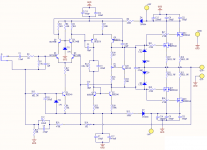
C10 is required under some load conditions
without it it does oscillate at times.
What is not rquired is the zobel network on the output.
I have sold thousands of these AV400 modules with this schematic over the last 12 years and they have proven to be very reliable.
without it it does oscillate at times.
What is not rquired is the zobel network on the output.
I have sold thousands of these AV400 modules with this schematic over the last 12 years and they have proven to be very reliable.
Stanley
Q10 on your PCB will not be reliable in that position.
The mosfets will thermally runaway.
This device must be mounted on top of one of the output devices.
to work well.
Q10 on your PCB will not be reliable in that position.
The mosfets will thermally runaway.
This device must be mounted on top of one of the output devices.
to work well.
Hi The Saint,
q10 won't work in that position (between the two pairs), why?
Is it time lag between output transistor temperataure change to sensor temp change?
or
is it reduced temperature swing from output devices to sensor?
or
something else?
q10 won't work in that position (between the two pairs), why?
Is it time lag between output transistor temperataure change to sensor temp change?
or
is it reduced temperature swing from output devices to sensor?
or
something else?
Hi Andrew
Q10 in this design running at +-70 volt will have thermal tracking issues when driving 4 Ohm loads if Q10 is not mounted on top of one of the output devices or even better mounting it onto a bar that is clamped across the output stage, At idle it will sit there quite happily.and I suspect with stanley's PCB layout running on 54 volts it most likely will not have any problems either.
However the 0.22 Ohm source resistors were chosen as a compromise between stability and power delivery.
meaning the amount of power wasted across the source resistors
into low impedance loads.
Vertical Mosfets are very easy to stablize at voltages below +-70v
above that, the Gate voltage threshold changes much more rapidly and is harder to thermally track with a Vbe multiplier mounted anywhere other than on top of one of the output devices. Others of you may have different experiences and I would be happy to here them, but this has been my experience.
It can be slowed down quite a bit by increasing the source resistors to 0.47- 0.68 ohms but in a high powered amplifiers this causes way to much wastage in power.
A way of getting around this is to add more output devices, but then more PCB real estate and other issues.
One of my latest designs uses 8 x IRFP260N devices in the output stage and is capable of 1kw into 4 Ohms.
once again I found a compromise of 0.33 Ohms as source resistors and the Vgs multiplier had to be mounted on top of the output stage devices anywhere else and it would not track well at all. The multiplier also had to be modified with MJE340s wired as diodes and connected in series with the resistor divider network. the MJE340s were also mounted on 2 other output devices. with this arrangement the bias does not shift at all under any load, it is rock solid even into 2 Ohm loads.
So I guess in a long winded way
I have answered your question😀
Hi The Saint,
thanks for that long explanation and your time.
It sounds from the description of the solutions that it is a temperature thing and not delay/lag.
Surprised the clamping bar is effective, I would have thought that was worse than using the heatsink, but just goes to show that intuition can be misleading.
Could part of the problem be undercompensation from using Vbe multiplier for FETs when maybe Vgs might be more appropriate, particularly when noting your observation that adding transistor strapped diodes (increased compensation factor) works well?
If this schematic should be used for lateral fets. Then I suspect the bias circuit needs to be altered.
The reason I am asking is that i have 2 rods of buzz lateral fets
cheers Michael
The reason I am asking is that i have 2 rods of buzz lateral fets
cheers Michael
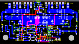
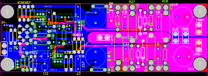
Hi Stanley,
the feedback trace and the output are taken from opposite ends of the common output trace.
Change it!!!!
the feedback trace and the output are taken from opposite ends of the common output trace.
Change it!!!!
C5 & C6 are in the wrong place. They are bypass caps and should be beside the V+ and V- of the main current changing semiconductors. Not on the end of a long leg miles (I exaggerate) away from where the current changes.
There is room next to the gate resistors to get small caps in here.
You could even put in a pair for each rail.
You could add an extra pin location on the signal ground to connect both the screen ground from the input RCA and to the central audio ground.
There is room next to the gate resistors to get small caps in here.
You could even put in a pair for each rail.
You could add an extra pin location on the signal ground to connect both the screen ground from the input RCA and to the central audio ground.
Hi,
one can connect the signal ground to central audio ground (CAG) by either taking the RCA input ground to CAG or taking the PCB signal ground to CAG. The extra pin allows the second option.
one can connect the signal ground to central audio ground (CAG) by either taking the RCA input ground to CAG or taking the PCB signal ground to CAG. The extra pin allows the second option.
Sorry this is not for hijacking the thread. But does anyone have a clue how this circuit would perform with Lateral Fets. such as BUZ 901's 906's as i have numerous matched pairs. (bought for a Tube-mosfet hybrid). They may serve good purpose in this schematic.
Thanks
Thanks
To AndrewT:
sorry, but I still don't understand. What is the difference between signal ground and central audio ground?
sorry, but I still don't understand. What is the difference between signal ground and central audio ground?
Stanley Drake said:To The Saint:
Do I need to improve something more or its schematics is absolutely right?
Can I use BC546C instead of BC546B? Does it improve performance?
For Q1 and Q2 BC546C are recommended but for Q3 and Q4 BC546A (less beta) are advisable because usually with less beta are a bit more rugged for Vce (imho at least) and less sensitive to Early effect. However not a thrilling affair... 😉
Hi
Piercarlo
Hi Stanley,
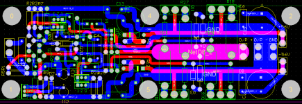
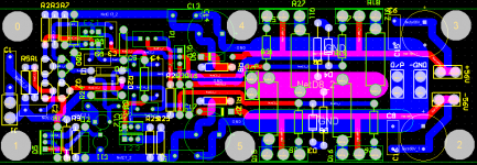
go back to the post1 schematic.
J1, the input plug has signal and signal ground.
This signal ground is connected to the Input screen, the RF filter return, the NFB and on this particular amplifier, the CCS (note that the negative power rail is trying to contaminate the signal ground via r13).
The labels GND are the power ground connections. These are dirty grounds that must be kept separate from the signal, until they are referenced to 0Volt.
The 0v reference is the central audio ground (some call it the star ground). It can be anywhere, on the PCB, or floating in the mid air at some central location or adjacent to the power supply common. It is NEVER on the common link between the smoothing capacitors.
Bring all the returns and grounds to the CAG (star). Some of these routes can be long and necessarily have inherent inductance. The resistor r24 is a short low inductance PCB link between signal ground and power ground that parallels the wire links to the CAG. If the resistor were zero ohms one would have an earth loop, creating hum.
Some PCB designers put the CAG on the PCB, but to simplifiy the wiring and connections they common many of the return lines before they reach the CAG. If the CAG is on the PCB then it needs to be star connected with about 6 or 7 separate wires coming from the various parts of the amplifier and off board returns. This looks untidy and is quite complicated to wire up (a computer style Dplug would solve this but I have never seen it done). I try to place all the gounds (PCB signal, PCB power, PSU common, and speaker/Zobel return) close together and put the CAG in a central location to minimise the wire lengths.
- Status
- Not open for further replies.
- Home
- Amplifiers
- Solid State
- A. Holton AV400 power amplifier