Member
Joined 2009
Paid Member
I always fancied building a DB output stage after following the Krill thread. Haven't decided yet if it will be the Krill or some other incarnation of the DB. I swore off designing new amplifiers so I'm looking to proudly borrow from an existing design approach and there were plenty of good reports on the Krill amp. However, I'm not sure I will take the risk of leaving out the Re. Or maybe I will 😀
Bigun,
I designed and sold a DB amp.
It sounded very good despite high levels of distortion, um, harmonics......
It used a variable CCS which increased in step with current in the output devices.
Had to use emitter resistors however to ensure stable quiescent......
Hugh
I designed and sold a DB amp.
It sounded very good despite high levels of distortion, um, harmonics......
It used a variable CCS which increased in step with current in the output devices.
Had to use emitter resistors however to ensure stable quiescent......
Hugh
Member
Joined 2009
Paid Member
I remember you mentioned that, I think Elvee had a crack at the variable current and the good old Audio Research D400A. My attempts to simulate something fancy like that never worked out.
You could transplant your variable CCS into the classic JLH'69, that would be a cool project.
You could transplant your variable CCS into the classic JLH'69, that would be a cool project.
My head is currently exploding, looking at various buffer ideas...
...stumbled into this one.
Hugh, that's not quite the same as Elvee's circuit... which may account for the apparently poor simulation, or perhaps some device model is tainted?
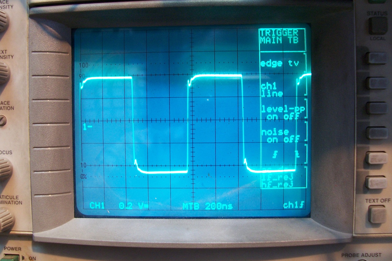
Looking back at the real world square wave, I'm worried about why the positive edge has some anomaly, while the negative looks very nice. I'd want both sides to look the same. Is it an artifact of the input signal or something else??
I'm personally fond of what I call "cross coupled" buffers... move two symmetrical connections from the usual diamond layout and you have it.
_-_-
...stumbled into this one.
Hugh, that's not quite the same as Elvee's circuit... which may account for the apparently poor simulation, or perhaps some device model is tainted?
Looking back at the real world square wave, I'm worried about why the positive edge has some anomaly, while the negative looks very nice. I'd want both sides to look the same. Is it an artifact of the input signal or something else??
I'm personally fond of what I call "cross coupled" buffers... move two symmetrical connections from the usual diamond layout and you have it.
_-_-
Hugh, that's not quite the same as Elvee's circuit.
_-_-
Yeah. What happens if you take out the current sources and put the original bootstrap in, pitch the emitter resistors?
Last edited:
Member
Joined 2009
Paid Member
Maybe the simple option is to wiggle the CCS up and down based on current through the load like Hugh describes - it's not much of a stretch to see it as a Nelson Pass Aleph as a driver stage.
Well, I am afraid I don't have any inverting buffer ready: lots of non-inverting, but not a single inverting.Elvee, I need a buffer, but inverting one with or without global NFB. Important is to have low distortion and to be quite simple. I simulated one in mine GainWire mk3 thread, but I am not very satisfied with it, to complicate. Do you have any good idea?
Damir
I'll think about it though, maybe a good idea will pop up
I am perfectly aware of that effect, I should rather say painfully aware, because it works in the wrong direction, and that's one of the things that is bugging meIs there something here (Bob Pease) ?
"If you need to know the tempco of VBE, it normally changes - 200 uV/degree C every time the current is reduced by a factor of 10."
What's All This VBE Stuff, Anyhow? nsc03943 - Datasheet Archive
They dissipate too much for that: without a good thermal connection to real heatsink, they would melt downdid you / can you try placing the drivers not on the heatsink but on top of the power devices so that they sense the temperature of the power device directly ? - they would run hotter of course but are essentially still being cooled by the heatsink via a 'hot' washer !
That is broadly my opinion too: the high temperature of the drivers provides some kind of "phase advance reserve" for the thermal compensation.The high driver current is the key, as they are pre-empting any temperature rise in the output stage. I suspect that if you did the same in a conventional bias spreader and made it into a significant heat source, it would work the same.
I think that this technique would fall down if the output transistors power dissipation was considerably higher than the bias spreader though, but happy to be proved wrong.
I have to say that I have seriously abused the prototype, to see if a brutal thermal excursion in the OP devices could trigger a thermal runaway, but apparently it didn't.
There is a bit of reflection in the cable leading to the function generator, and what you call "anomaly" is in in fact normal, for the first oscillogram:Looking back at the real world square wave, I'm worried about why the positive edge has some anomaly, while the negative looks very nice. I'd want both sides to look the same. Is it an artifact of the input signal or something else??
The second oscillogram shows the situation with a much reduced bias current, which means the apparently "clean" side is now slew-limited, which means it polishes off the small details of the signal it is unable to track.
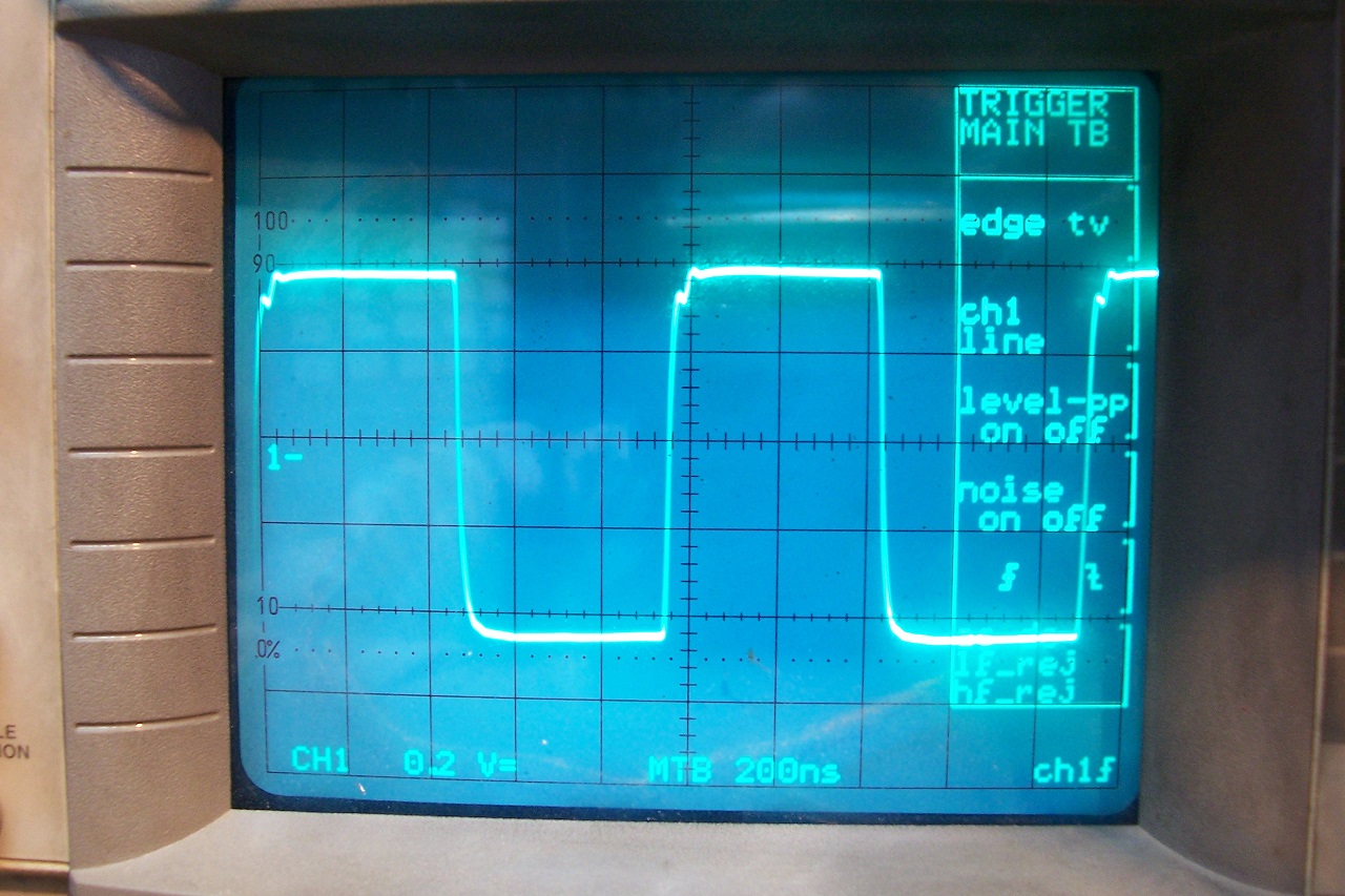
Note that the timebase setting is 200ns/div....
Well, I am afraid I don't have any inverting buffer ready: lots of non-inverting, but not a single inverting.
I'll think about it though, maybe a good idea will pop up
....
I simulated this inverting buffer, but I would like to have something simpler. With high impedance inverting input. http://www.diyaudio.com/forums/soli...e-amp-very-low-distortion-19.html#post4888037
Damir
The slew limiting at lower current doesn't bother me, and thanks for the explanation.
Also, I did 'note' the scary fast timebase setting! 😀
Wondering why, just curious, why the negative side seems to slew limit before the positive - not that it matters much...
Given the caps in the circuit, what effects are there at very low frequencies, if any?
And did you test the real circuit with an FFT to see what it is actually doing??
_-_-bear
Member
Joined 2009
Paid Member
If single driver - single output is thermally stable, do you think it would stretch to a darlington driver - darlington output ?
Complementary transistors are more an article of faith than the reflection of physical reality: with silicon, it is an impossibility, which means that one member of the pair will always have larger capacitances, lower Ft, different Hfe, etcWondering why, just curious, why the negative side seems to slew limit before the positive - not that it matters much...
The usual effects for bootstrapping schemes: at low frequencies, the simulated current sources will degenerate into plain resistances, which will affect the output drive amongst other things.Given the caps in the circuit, what effects are there at very low frequencies, if any?
The good news is that you can extend the low frequency limit by any arbitrary amount, because given the resistors values, it doesn't require huge caps to do so.
Anyway, CCS's could be used instead.
No, but there again it's probably very much like any other diamond OPAnd did you test the real circuit with an FFT to see what it is actually doing??
I wouldn't hazard a guess on that: it is too much of a stretch. IMHO, an actual physical test is the only way to get a reliable answerIf single driver - single output is thermally stable, do you think it would stretch to a darlington driver - darlington output ?
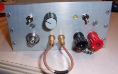
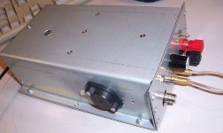
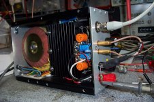
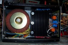
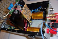
Here it is, shoe-horned into a satisfyingly compact skin.
It also includes a supply, based on overcurrent protected capacitance multipliers (without emitter resistors, the protection would be difficult to include in the buffer itself), and a high-impedance input amplifier adjustable from +6 to +20dB based on a LH0032.
The raw input impedance of the buffer is ~2.5K. It is accessible, because the LH0032 is incapable of matching the voltage swing and bandwidth of the buffer: 5.5MHz, both for small & large signal.
It could operate as a power video amplifier or a SW transmitter.
The THD@14W, 1KHz is 0.075%, and remains practically constant at lower power levels (that is obviously without GNFB, by definition)
Attachments
- Status
- Not open for further replies.
- Home
- Amplifiers
- Solid State
- A diamond paradox?