Thanks to the JFET noise measurements by Scott Wurcer, we know that the famous 2SK170 is not the lowest noise JFET available. In fact, both the 2SK369 and especially the underrated 2SK372 is significantly better.
http://www.diyaudio.com/forums/pass-labs/175040-more-fet-noise-measurements-euvl.html
The 2SK372 has a TO-92 equivalent, the 2SK363, which according to datasheet has a higher power rating. However, this is only true if the JFET is used free standing, i.e. dissipating to ambient by free convection. As we shall see, the smaller package of the 2SK372 has a sizable advantage when used as a coupled pair and together with a heat sink.
For the old workhorse, the current source loaded JFET source follower, recently reincarnated as the Pass B1, the following characteristics of the active device would be desirable:
1) high transconductance (for low output impedance),
2) low thermal resistance between the 2 devices (for best thermal tracking and low DC offset),
3) high Idss (for better linearity and current driving capability),
4) well matched Idss (for low DC offset at null signal),
5) low Cgd (for high bandwidth).
The 2SK389 in V grade is undoubtedly the best solution for criteria 2 to 5, only if you can still get them. Compared to the 2SK170 in TO92, 2SK372 scores on at least two counts. Its transconductance is about 2x that of the 2SK170, and its smaller package size means that when glued face to face with silver epoxy, the 2 silicon dies have a smaller physical distance between them and hence better thermal coupling. High Idss can be obtained by using the V grade (on average 20mA), but that also means higher dissipation, and hence the necessity of a heat sink so that reliability does not suffer. The 2SK372 does have a higher Cgd, but with 15pF still gives a 10MHz bandwidth with 1k ohm source impedance, so no real issue.
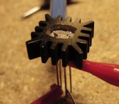
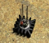
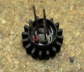
For thermal coupling, the most obvious is to glue the 2 devices face to face at their flat faces. This also provides a convenient connection for the source pin of the top device (the follower) to the drain pin of the bottom device (the current source). The gate pin of the bottom device can also be shorted to the source pin directly at the package (see photo), leaving only 4 external connections to the outer world -- +Vs, -Vs, input and output.
The thermal coupling can however be further increased by wrapping the outer surfaces of the coupled devices with a metal ring of sufficient thickness. This increases the gluing surface of the devices (the glue and the JFET package encapsulation are the highest resistance in the thermal coupling path), and hence reduce thermal resistance. Aluminium has a thermal conductivity > 10x that of silver epoxy, so that one can treat the thick aluminium ring as a thermal short circuit.
It is only natural that we make a heat sink out of the “ring”. We have tested 2 designs, a rectangular one measuring 10x10x4mm, and a cylindrical design of 8mm diameter and 6mm high.
The rectangular version is glued with 2x 2SK372V of Idss 21.82mA and 22.37mA respectively (these are my matching rejects and is used here for thermal design verification). Using supply rails of +/-9V, the steady state heat sink temperature was measured at 44°C, and the output DC offset at -6.5mV. The output DC meets expectation, and it shows that even a 0.3mA mismatch will cause measurable DC offset (even more for 2SK170s with its lower transconductance). The thermal resistance of the heat sink is calculated to be 57°C/W, not bad at all for such a small heat sink. Ambient temperature was 20°C. But more importantly, the temperature of the JFET die, calculated to be about 70°C, is low enough now to ensure reliability even when we are dissipating about 200mW per device. The DC offset remains constant to 0.1mV from cold start to steady state, confirming the very effective thermal coupling of the 2 devices.
The cylindrical version has even better performance, though quite a bit more difficult to manufacture. Using 2x 2SK372V with Idss of 21.82mA and 22.37mA, the DC offset was measured at -8.7mV, and the steady state sink temperature at 48°C. This corresponds to a thermal resistance of 48°C/W for the cylindrical heat sink.
All in all, the solutions shown here provide a compact, high-performance source follower which can find many useful applications such as Sallen Key filter buffers, CD IV converter output buffers, etc., at a very moderate cost. There is IMHO no good reason not to use these instead of connecting opamps as unity gain buffers.
Patrick
http://www.diyaudio.com/forums/pass-labs/175040-more-fet-noise-measurements-euvl.html
The 2SK372 has a TO-92 equivalent, the 2SK363, which according to datasheet has a higher power rating. However, this is only true if the JFET is used free standing, i.e. dissipating to ambient by free convection. As we shall see, the smaller package of the 2SK372 has a sizable advantage when used as a coupled pair and together with a heat sink.
For the old workhorse, the current source loaded JFET source follower, recently reincarnated as the Pass B1, the following characteristics of the active device would be desirable:
1) high transconductance (for low output impedance),
2) low thermal resistance between the 2 devices (for best thermal tracking and low DC offset),
3) high Idss (for better linearity and current driving capability),
4) well matched Idss (for low DC offset at null signal),
5) low Cgd (for high bandwidth).
The 2SK389 in V grade is undoubtedly the best solution for criteria 2 to 5, only if you can still get them. Compared to the 2SK170 in TO92, 2SK372 scores on at least two counts. Its transconductance is about 2x that of the 2SK170, and its smaller package size means that when glued face to face with silver epoxy, the 2 silicon dies have a smaller physical distance between them and hence better thermal coupling. High Idss can be obtained by using the V grade (on average 20mA), but that also means higher dissipation, and hence the necessity of a heat sink so that reliability does not suffer. The 2SK372 does have a higher Cgd, but with 15pF still gives a 10MHz bandwidth with 1k ohm source impedance, so no real issue.
For thermal coupling, the most obvious is to glue the 2 devices face to face at their flat faces. This also provides a convenient connection for the source pin of the top device (the follower) to the drain pin of the bottom device (the current source). The gate pin of the bottom device can also be shorted to the source pin directly at the package (see photo), leaving only 4 external connections to the outer world -- +Vs, -Vs, input and output.
The thermal coupling can however be further increased by wrapping the outer surfaces of the coupled devices with a metal ring of sufficient thickness. This increases the gluing surface of the devices (the glue and the JFET package encapsulation are the highest resistance in the thermal coupling path), and hence reduce thermal resistance. Aluminium has a thermal conductivity > 10x that of silver epoxy, so that one can treat the thick aluminium ring as a thermal short circuit.
It is only natural that we make a heat sink out of the “ring”. We have tested 2 designs, a rectangular one measuring 10x10x4mm, and a cylindrical design of 8mm diameter and 6mm high.
The rectangular version is glued with 2x 2SK372V of Idss 21.82mA and 22.37mA respectively (these are my matching rejects and is used here for thermal design verification). Using supply rails of +/-9V, the steady state heat sink temperature was measured at 44°C, and the output DC offset at -6.5mV. The output DC meets expectation, and it shows that even a 0.3mA mismatch will cause measurable DC offset (even more for 2SK170s with its lower transconductance). The thermal resistance of the heat sink is calculated to be 57°C/W, not bad at all for such a small heat sink. Ambient temperature was 20°C. But more importantly, the temperature of the JFET die, calculated to be about 70°C, is low enough now to ensure reliability even when we are dissipating about 200mW per device. The DC offset remains constant to 0.1mV from cold start to steady state, confirming the very effective thermal coupling of the 2 devices.
The cylindrical version has even better performance, though quite a bit more difficult to manufacture. Using 2x 2SK372V with Idss of 21.82mA and 22.37mA, the DC offset was measured at -8.7mV, and the steady state sink temperature at 48°C. This corresponds to a thermal resistance of 48°C/W for the cylindrical heat sink.
All in all, the solutions shown here provide a compact, high-performance source follower which can find many useful applications such as Sallen Key filter buffers, CD IV converter output buffers, etc., at a very moderate cost. There is IMHO no good reason not to use these instead of connecting opamps as unity gain buffers.
Patrick
Attachments

Last edited:
Has any of the Linear Systems parts been tested to see if they really are low noise as claimed? It seems that the LSK389 would be a viable part if so since you can buy them quite easily.
There is an article on noise of LSK389 :
http://www.audioxpress.com/magsdirx/ax/addenda/media/colin2993.pdf
But if I remember correctly, someone some time ago posted a comment that JFETs from Linear Systems was not consistent in quality.
I have not use many of them, so no idea.
As someone who has worked in the semiconductor industry for over 25 years, I know how critical manufacturing processes are, and I simply do not believe a small company like Linear Systems would have the same resources at their disposal as Toshiba, or Philips for that matter. So I shall use Toshiba, Philips (NXP), Onsemi, .... , as far as I can.
You can say I am biased. I guess I am.
Patrick
yeah the main ones that interest me from linear are the small sot23 versions, more great and informative research Patrick, yet another reason for me to buy some of your sinks. hoping you still have some left, I have emailed you friend
I asked Linear Systems multiple time for SOT23.
I don't think they keep them in stock, which means you need to order a packaging lot (10k ??).
Patrick
I don't think they keep them in stock, which means you need to order a packaging lot (10k ??).
Patrick
I asked Linear Systems multiple time for SOT23.
I don't think they keep them in stock, which means you need to order a packaging lot (10k ??).
Patrick
I will be measuring all the Linear System's parts after I build rev 2 of my test setup. I looked at one LSK170 and it was actually slightly worse but remember these measurements are higher res than reading an analog meter.
I hope to hear more details from you about your revision 2 (when finished), so that I can also repeat the tests and perform similar measurements on other JFETs.
Hopefully in the end we'll have a collection of measurement of a wide range of JFETs.
My sincere thanks for your work up to now.
Patrick
Hopefully in the end we'll have a collection of measurement of a wide range of JFETs.
My sincere thanks for your work up to now.
Patrick
Hi Patrick,
Do you have plans to produce either of these heatsinks for sale and public consumption?
Thanks,
Dave
Do you have plans to produce either of these heatsinks for sale and public consumption?
Thanks,
Dave
If there is sufficient interest we shall make them available. Most likely only the square version, as the round version with the recess at the back etc. is quite a bit more machining, and cost more than double.
We shall start making them for a minimum demand of 100 pieces, and as before min 10pcs, over 25pcs no 5Euro surcharge, price probably around 2.50 to 3.00 Euros because of small batch. But we need to know quantities first.
(We shall change to Euro from now on as US dollar is a very unstable currency.)
If you volunteer to try 2SK372V and promised to report back, I have a few here to send you right now.
Patrick
Someone just placed an order for 50 pcs. Anyone else wants to join before I send drawings off for production ?
If you are in the US and want small quantities, you might consider group buying with him. I guess I can get that arranged.
Patrick
If you are in the US and want small quantities, you might consider group buying with him. I guess I can get that arranged.
Patrick
I too follow this thread closely. Seems I can get 48 pc 2SK363 for 0,80 euro here (Western Europe) and no shipping fee. Dunno about the grade though. So, I wait for the "good buffers" with the special sinks, how much for them TO92 sinks only ? Is it easy to glue all this correctly into the sinks then let dry ?
Thanks for info 🙂
Brds,
nAr
Thanks for info 🙂
Brds,
nAr
You might not need a sink for TO92 if you are using BL grade.
They have a higher dissipation rating, and if BL lower current / dissipation.
I do not currently have a design for TO92, so we'll have to specially design one for you if you want.
Patrick
They have a higher dissipation rating, and if BL lower current / dissipation.
I do not currently have a design for TO92, so we'll have to specially design one for you if you want.
Patrick
You might not need a sink for TO92 if you are using BL grade.
I don't know the grade yet ... I think the stock is NOS, ordered 50 pieces to see what I can do with them 😀
nAr
EDIT: found some nice 2SK147 BL in my electronic rubbish. I might have only 4 pieces of them 🙁
Got my 2SK363 from NOS, BL grade, Toshiba, 48 pcs at 0,70€/pc 🙂
Time for experiments ? 😎
Brds,
nAr
Time for experiments ? 😎
Brds,
nAr
What else ?
First match, then glue, then power up and measure DC offset with input grounded.
And then you are in business.
No need heatsink for 363BL.
Patrick
First match, then glue, then power up and measure DC offset with input grounded.
And then you are in business.
No need heatsink for 363BL.
Patrick
Sorry to bump in so quick, not to be rude, but which schematic do you consider ? B1 style or even simpler (followers suitable for active crossovers ?)
Regards,
nAr
Regards,
nAr
http://www.borbelyaudio.com/adobe/ae699bor.pdf
Figure 15C, change Rs to zero (no resistor), rail voltages +/-9V to +/-12V.
Read post #1 and look at the photos carefully.
Patrick
Figure 15C, change Rs to zero (no resistor), rail voltages +/-9V to +/-12V.
Read post #1 and look at the photos carefully.
Patrick
Post #1 shows you how to hard wire, so that you are left with 4 wires for the outside world -- +Vs, input, output, -Vs.
Pls report back after listening test.
P.
Pls report back after listening test.
P.
Last edited:
- Status
- Not open for further replies.
- Home
- Amplifiers
- Solid State
- A Compact, High-Performance Source Follower Module