Pushbutton
For our pushbuttons, we will use something like the E-Switch LP4OA1PBCTW:
- Momentary function
- Vertical PCB mount (to make it easier to mount the PCB on the cover)
- Black housing (white makes it much harder to source the parts)
- Round cap without bezel
- Transparent cap
- White LED color
For our pushbuttons, we will use something like the E-Switch LP4OA1PBCTW:
- Momentary function
- Vertical PCB mount (to make it easier to mount the PCB on the cover)
- Black housing (white makes it much harder to source the parts)
- Round cap without bezel
- Transparent cap
- White LED color
Last edited:
Brick Submodule Interconnect
Of all the bricks that we need to develop, the 1 × 1 bricks offerings buttons, encoders, and ports are the most important, and because we've decided to build them around the following submodules, we need to design a simple interconnect between a brick's microcontroller board and its (up to four) submodule boards:
- B3: three buttons
- B4: four buttons
- E2: two encoders
- E3: three encoders
- E4: four encoders
- P3: three ports
- P4: four ports
Buttons are the simplest and simply require two IOs: one for the switch and one for the LED. While we could use eight IOs to drive a 4-button submodule, it's probably best to use an SPI port and a pair of shift registers, because we'll need the SPI port for other submodules anyway.
An encoder with RGB illumination requires 5 × IOs and +5V, and we need up to three of them on a submodule (our 4-channel small encoder submodule won't use illuminated encoders). Again, with such a large number of IOs, we're probably best using an SPI port in combination with some shift registers.
Last but not least, our ports will need the following:
- 4 × IOs for the 4-LED circuit board indicator
- 1 × IO for audio input signature
- 1 × IO for audio output signature
- 1 × ADC for CV input signal
- 1 × IO for CV output signal
- 1 × IO for CV input signature
- 1 × IO for CV output signature
There, we should probably use an SPI port and 4 × ADC lines, alongside some shift registers and a 16-channel LED driver.
Once we factor all this, it become apparent that our interconnect should provide the following:
- 4-pin SPI port
- 4 × ADC lines
- +5V
- GND
This gives us a total of 10 pins. But in order to support future enhancements, we might want to consider using a 12-pin interconnect, just in case. Also, this design assumes that we might use up to 16 × ADC channels (for the P16 16-port brick). With that in mind, we are currently looking at more powerful microcontrollers, such as the STM32F373VC. This would be a major upgrade from the ATxmega32A4U, but it might not be such a bad idea.
Modern converters are all clocked from MCLK directly and the I2S data is probably clocked into shift registers / buffers. I don't see how levels of jitter that don't violate the setup and hold timing or something crazy like that could have an impact on those signals since they aren't the conversion clock.
As far as I am aware most modern converters use the bit clock as the timing reference, as far as jitter is concerned, for the conversion of data from A>D or D>A.
The master clock itself is only used to allow the oversampling of Delta Sigma parts to function. Most chip manufacturers state that the master clock needs to run synchronously to the other clocks but the phase relationship between them is not important. Data transfer and audio timing is managed by the rate of the bit clock.
This only applies to an ADC operating in slave mode though. If the ADC is operating as a master then you only need supply it with a master clock and the chip will generate everything else.
Some DACs, mostly the ESS parts, have built in ASRCs that reclock the data to a provided high quality master clock. This eliminates jitter problems that would ordinarily occur from high jitter being present on the incoming bit clock, or any other incoming clock, but the flow of data is still controlled by the incoming bit clock.
Given the system at hand the master for all data flows should ideally be the USB interface. It would therefore take two low jitter master clock sources, such as the NDK parts, one for 44.1k base data rates, one for 48k base data rates and their multiples.
The USB interface would then produce buffered master, bit and LR clocks, plus the relevent data lines. These would then interface with the DSP core or be sent directly to the audio converters.
For example if going to a DAC the data would first pass through the DSP before being converted. But if going to an ADC, the master clock, bit clock and LR clock would be fed directly to the ADC. The ADC would then output a data stream and this, along with the bit and LR clock would be fed into the DSP, for processing, before the data line be fed, from the DSP, into the USB interface.
If the system of this thread is only going to use analogue inputs and outputs then you're done as the data rates are all handled directly by the USB interface and everything is synchronous from bringing to end. The problem occurs when you want to add in digital inputs. Outputs are fine as they are just slaved to the internal clocks (connecting a SPDIF transceiver, instead of a DAC, to an output data line is essentially the same thing). But inputs come with their own timing/clock and require special attention. Realistically though the answer is simple you have to use an ASRC on the incoming digital data stream then use one of the USBs digital input data ports as the master for the signals that the ASRC reclocks to.
The critical clock is definitely MCLK for every single delta sigma part. It wouldn't even be possible for the part to function if the conversion clock was BCK. If you find or look at detailed enough block diagrams you'll see this. I'm not sure what would lead you to believe the bit clock is of any importance? It is only important in cheap parts that do not have an MCLK input and recover it via PLL or in obsolete DACs like PCM1704.
In such a complex system as this, it is probably best to have an I2S master in the FPGA and everything else that can, including the USB interfaces, operate in slave mode. Obviously, SPDIF inputs can't operate like this and will need a PLL, FIFO, or ASRC to be synchronized with the clocks in the box. I already described, perhaps in different words, the need to bridge clock domains for digital sources that come with their own master clocks. You don't absolutely have to use an ASRC to do this.
Last edited:
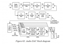
Just as an example, this attachment is from an early 2000s Cirrus Logic ISSCC paper describing some unknown delta-sigma audio DAC design. You can see that the converters are actually clocked at 256*Fs, which is higher than the bit clock will ever be, and a typical value for MCLK.
Attachments
In such a complex system as this, it is probably best to have an I2S master in the FPGA...
The I2S master will indeed be in the FPGA.
And yes indeed, I want the system to be able to mix both analog and digital inputs, and the latter will need to be synchronized somehow. I am still digesting what you sent earlier on that topic...
Thanks!
As far as I am aware most modern converters use the bit clock as the timing reference, as far as jitter is concerned, for the conversion of data from A>D or D>A...
Thanks a lot for all this. Super helpful!
Stick PCB Orientation
With our latest design, our system offers three distinct levels of modularity:
- Grid-level: up to 8 grids connected together over USB
- Brick-level: up to 16 bricks connected to a grid over USB
- Stick-level: up to 4 sticks mounted in a brick over SPI and ADC
What we now call "sticks" are the submodule PCBs like these:
- B3: three buttons
- B4: four buttons
- E2: two encoders
- E3: three encoders
- E4: four encoders
- P3: three ports
- P4: four ports
Our original plans for these sticks was that some would be mounted parallel to the brick's cover, and some perpendicular to it. After further evaluation, we believe that we should mount all of them perpendicular to the cover. There are several reasons for that:
First, it will simplify the overall design (the less variations, the better).
Second, it will make it easier to cram all the components that some sticks might need. This is important, because most sticks contain components like buttons, encoders, or ports that are mounted on the PCB with through holes, and several high-density sticks pack these components quite tightly, leaving very little space for anything else.
Fortunately, our bricks will have to be quite tall (probably 60mm to make a perfect cube), because the Bourns PSP are 47.2mm tall. Therefore, while we will we be space constrained horizontally, we will have plenty of space vertically, and we should put it to good use.
To do so, we will need to ensure that all our buttons, encoders, and ports can be securely attached to the brick's cover using nuts, and that they can be mounted on the PCB with the right orientation. The STX-3150-3N-1 is perfect for that, but the encoder that we had selected would not work.
Instead, we could use something like the DPL12SH2424A21F1, which is small enough to be used for both small and large encoders (only the knob cover would change). This encoder is dual-color only (no RGB), but that should be plenty enough.
The only missing part is the switch, but I'm pretty sure that we'll find a suitable one. And if we don't, we'll use a regular switch and add some mounting brackets on the PCB.
For the interconnect, we will use standard 2.54mm pins on the sticks and matching headers on the microcontroller board. This will make the assembly really easy and the BoM as affordable as can be.
Having so much vertical space will make it possible to add some interesting components on the sticks, such as a Korg Nutube amplifier for example. Also, with a single row of 2.54mm pins, we could probably have 20 of them, allowing us to provide an extra set of 10 × IOs. This would reduce the need for shift registers on many stick boards. As a result, the interconnect would provide:
- 4-pin SPI
- 4 × ADC lines
- 10 × IOs
- GND
- +5V
- -5V
- Unused pin
Of course, 60mm is quite tall for these bricks, but we need to keep in mind that the back of our grids will be quite tall as well, because we need to pack many PCBs onto a fairly tall stack. Therefore, making the bricks a bit taller will actually reduce the vertical gap between the main control surface and the displays of the single-board-computers that sit at the top of our tall stack.
The I2S master will indeed be in the FPGA.
And yes indeed, I want the system to be able to mix both analog and digital inputs, and the latter will need to be synchronized somehow. I am still digesting what you sent earlier on that topic...
Thanks!
No problem. You can basically slave the USB receiver if you have one and the network audio stuff, I think. Those can or do operate asynchronously and control flow via feedback to the host. So you can have the XMOS be an I2S slave and not worry about dropouts or clicks or anything.
For SPDIF, AES, ADAT, HDMI, etc there is no opportunity for feedback, so they have the clock encoded with the data and those receivers recover it. You don't really want to use the recovered clock directly (if you want state of the art performance) in many cases because it can be very jittery. ASRC's like the AD1896, SRC4392, AKM version, etc. will attenuate that jitter with a DPLL that has a very low corner frequency. Alternatively that CS2100 I think works like some of the TI jitter cleaners for LVDS.
That makes a lot of sense. I will look into the different options for an ASRC. If you were to build a statement device, which one would you pick?
Yes I am aware of that and jitter on the master clock is important for proper DAC operation and performance. But the data flow and data clocking is all synchronised to the bit clock/LR clock.
It has to be, by its very nature the data that encodes the analogue waveform is stored and retrieved by the rising edges of the bit clock. When a complete sample has been received the DAC process it and outputs it. The timing of the successive samples comes directly from the bit clock and nothing else.
DSPs don't even need the audio master clock to function. They need their own internal processing clock for data manipulation (very much like their own master clock) but the data itself is clocked in and then out again via the bit clock.
The master clock isn't needed for audio data or audio timing this is all present in the data stream, the LR clock and bit clock. Jitter within these appears on the output of a DAC because these are precisely what controls the flow of data.
The master clock in DS converters supplies the oversampling sections with the high speed clock required for device operation but the flow of data within them beats to the rhythm of the bit clock.
Of course the master clock needs to be low jitter too otherwise jitter introduced to the oversampling sections will appear on the output. But jitter present on the bit clock and data stream are very relevant.
TI say in the datasheet for the pcm1792a
In other words the LR clock (and by extension bit clock and data stream) needs to run at an exact division of the master clock with regards to frequency but not with regards to phase. This means the DAC doesn't need the rising edges of the master clock to coincide with the rising edges of any of the other clocks. As a result none of the timing of the audio data is tied to the master clock and it's tiny changes within the timing of the data samples on the rising edges of the data/LR/bit clock that results in jitter on the output of the DAC.
In fact all ASRCs and the jitter eliminator within the ESS DACs are about getting rid of jitter present within the data clocks and not the master clock. They don't even need the master clock of the original data line to function because it serves no purpose.
In ESS' white paper on their sabre DACs, towards the end they say this...
This has nothing to do with the master clock as they are showing how effective the ESS part is at removing the jitter present on the incoming data line. And without that jitter removal, no matter how jitter free your master clock might be, if there's jitter on the data clocks your DAC performance suffers.
Old multibit DACs didn't need a master clock because they didn't oversample the data they just ran at the rate of the data itself. They were however susceptible to jitter present within the data clocks, they had to be these were the only clocks they used and jitter didn't just vanish as a physical property because they didn't use a master clock.
DS are more susceptible to problems with jitter precisely because they use a master clock. They will show performance degradation towards jitter present on both the master clock and the data clocks. But, as far as I am aware, are also worse at suppressing jitter present within the data clocks than multibits were. A guess would assume this is because of the oversampling process where small timing/jitter issues in the data clocks are magnified by the oversampling process and then modulated by any jitter on the master clock.
All clocks need to be jitter free.
As to what hardware part operates as the master device. The DSP doesn't make much sense. The DSP processing core will most likely run asynchronously to the actual data clocks anyway. Typically a data byte will be clocked into the DSPs front end. Upon receiving this the DSP will process the data byte as fast as possible and then present it to the DSPs back end. When the next LR clock pulse comes along the data is clocked out with the rising edges of the bit clock. Of course the DSP can delay the outputting of the data by X sample periods if necessary (for delay stages) but usually a DSPs audio capability is determined by how much data is can process in one sample period, be it 44, 48, 96 or 192kHz. Once the processing would take longer than one sample period you've gone beyond what the DSP can do in real time.
Data processing in the DSP core runs at the rate of the DSPs internal clock, most likely from an internal PLL and at many MHz maybe even GHz. It has no relationship with the audio clocks, except for the fact it starts number crunching the instant it receives an audio data byte. It has no use for an audio master clock itself and its internal clock jitter has absolutely no bearing on the jitter on its output because that is clocked and timed to the LR/bit clock.
If you wanted you could provide the DSP/Xilinx chip with two high quality audio master clocks, one at 44.1k and it's multiples then one at 48kHz and it's multiples. Then have a part of the Xilinx chip work on clock generation. This would then feed the USB interface, DAC, ADC and DSP audio data input/output, but it would need a lot of interfacing between the USB interface and the Xilinx chip. You would also need bespoke USB interface code.
Having worked with a Cmedia asynchronous USB interface using it as a slave just seems like a massive mess. The chip itself has different audio input and output blocks such that you can have one DAC running at 44.1k whilst another runs at 96k, as well as having one ADC going at 192k and another at 88.2k. This is all at the same time. The operating conditions for each input/output block is handled via software via the operating system and is controlled by a software/hardware combination onboard the Cmedia chip.
With the USB interface acting as a master it takes the two high quality clocks (44.1 and 48k multiples etc) and generates all of the required clocks for whatever you want the chip to do. It's been designed specifically for this task and slaving the DSP audio input/outputs to the USB interface is just as easy as slaving it to clocks generated on one of its arm cores.
Slaving the USB interface to an external clock generation source within the Xilinx chip sounds like a nightmare, you'd need multiple clock lines for each input/output module along with communication between the USB interface, Xilinx chip and the operating system. I mean if the OS requests a sample rate change the USB interface needs to change its settings but the Xilinx chip needs to alter its clock generation settings to match too. Plus making it all work with ASIO.
This seems like a massive headache Vs just having the USB module act as a master and with drivers that already work.
If you really wanted to push the boat out you could ditch a third party USB interface entirely and use the USB port on the Xilinx chip. Have one of the arm cores handle the audio communication with the PC. That can then act as the audio master and feed everything directly. This is both elegant and simpler, requiring fewer chips and making PCB routing less complex. But it adds in a layer of complexity elsewhere. USB protocols are a pain and if someone you know is good with them then writing drivers and your own USB code may not be that hard
It has to be, by its very nature the data that encodes the analogue waveform is stored and retrieved by the rising edges of the bit clock. When a complete sample has been received the DAC process it and outputs it. The timing of the successive samples comes directly from the bit clock and nothing else.
DSPs don't even need the audio master clock to function. They need their own internal processing clock for data manipulation (very much like their own master clock) but the data itself is clocked in and then out again via the bit clock.
The master clock isn't needed for audio data or audio timing this is all present in the data stream, the LR clock and bit clock. Jitter within these appears on the output of a DAC because these are precisely what controls the flow of data.
The master clock in DS converters supplies the oversampling sections with the high speed clock required for device operation but the flow of data within them beats to the rhythm of the bit clock.
Of course the master clock needs to be low jitter too otherwise jitter introduced to the oversampling sections will appear on the output. But jitter present on the bit clock and data stream are very relevant.
TI say in the datasheet for the pcm1792a
The PCM1792A requires the synchronization of LRCK and system clock, but does not need a specific phase relation between LRCK and system clock.
In other words the LR clock (and by extension bit clock and data stream) needs to run at an exact division of the master clock with regards to frequency but not with regards to phase. This means the DAC doesn't need the rising edges of the master clock to coincide with the rising edges of any of the other clocks. As a result none of the timing of the audio data is tied to the master clock and it's tiny changes within the timing of the data samples on the rising edges of the data/LR/bit clock that results in jitter on the output of the DAC.
In fact all ASRCs and the jitter eliminator within the ESS DACs are about getting rid of jitter present within the data clocks and not the master clock. They don't even need the master clock of the original data line to function because it serves no purpose.
In ESS' white paper on their sabre DACs, towards the end they say this...
The lower plot (Figure 3) compares the jitter performance of a typical competitor’s part (red, or upper line) with the Sabre DAC (blue, or lower line). The graph shows THD+Noise vs. Frequency with only 2nS of random jitter on the data transport clock.
This has nothing to do with the master clock as they are showing how effective the ESS part is at removing the jitter present on the incoming data line. And without that jitter removal, no matter how jitter free your master clock might be, if there's jitter on the data clocks your DAC performance suffers.
Old multibit DACs didn't need a master clock because they didn't oversample the data they just ran at the rate of the data itself. They were however susceptible to jitter present within the data clocks, they had to be these were the only clocks they used and jitter didn't just vanish as a physical property because they didn't use a master clock.
DS are more susceptible to problems with jitter precisely because they use a master clock. They will show performance degradation towards jitter present on both the master clock and the data clocks. But, as far as I am aware, are also worse at suppressing jitter present within the data clocks than multibits were. A guess would assume this is because of the oversampling process where small timing/jitter issues in the data clocks are magnified by the oversampling process and then modulated by any jitter on the master clock.
All clocks need to be jitter free.
As to what hardware part operates as the master device. The DSP doesn't make much sense. The DSP processing core will most likely run asynchronously to the actual data clocks anyway. Typically a data byte will be clocked into the DSPs front end. Upon receiving this the DSP will process the data byte as fast as possible and then present it to the DSPs back end. When the next LR clock pulse comes along the data is clocked out with the rising edges of the bit clock. Of course the DSP can delay the outputting of the data by X sample periods if necessary (for delay stages) but usually a DSPs audio capability is determined by how much data is can process in one sample period, be it 44, 48, 96 or 192kHz. Once the processing would take longer than one sample period you've gone beyond what the DSP can do in real time.
Data processing in the DSP core runs at the rate of the DSPs internal clock, most likely from an internal PLL and at many MHz maybe even GHz. It has no relationship with the audio clocks, except for the fact it starts number crunching the instant it receives an audio data byte. It has no use for an audio master clock itself and its internal clock jitter has absolutely no bearing on the jitter on its output because that is clocked and timed to the LR/bit clock.
If you wanted you could provide the DSP/Xilinx chip with two high quality audio master clocks, one at 44.1k and it's multiples then one at 48kHz and it's multiples. Then have a part of the Xilinx chip work on clock generation. This would then feed the USB interface, DAC, ADC and DSP audio data input/output, but it would need a lot of interfacing between the USB interface and the Xilinx chip. You would also need bespoke USB interface code.
Having worked with a Cmedia asynchronous USB interface using it as a slave just seems like a massive mess. The chip itself has different audio input and output blocks such that you can have one DAC running at 44.1k whilst another runs at 96k, as well as having one ADC going at 192k and another at 88.2k. This is all at the same time. The operating conditions for each input/output block is handled via software via the operating system and is controlled by a software/hardware combination onboard the Cmedia chip.
With the USB interface acting as a master it takes the two high quality clocks (44.1 and 48k multiples etc) and generates all of the required clocks for whatever you want the chip to do. It's been designed specifically for this task and slaving the DSP audio input/outputs to the USB interface is just as easy as slaving it to clocks generated on one of its arm cores.
Slaving the USB interface to an external clock generation source within the Xilinx chip sounds like a nightmare, you'd need multiple clock lines for each input/output module along with communication between the USB interface, Xilinx chip and the operating system. I mean if the OS requests a sample rate change the USB interface needs to change its settings but the Xilinx chip needs to alter its clock generation settings to match too. Plus making it all work with ASIO.
This seems like a massive headache Vs just having the USB module act as a master and with drivers that already work.
If you really wanted to push the boat out you could ditch a third party USB interface entirely and use the USB port on the Xilinx chip. Have one of the arm cores handle the audio communication with the PC. That can then act as the audio master and feed everything directly. This is both elegant and simpler, requiring fewer chips and making PCB routing less complex. But it adds in a layer of complexity elsewhere. USB protocols are a pain and if someone you know is good with them then writing drivers and your own USB code may not be that hard
Yes I am aware of that and jitter on the master clock is important for proper DAC operation and performance. But the data flow and data clocking is all synchronised to the bit clock/LR clock.
It has to be, by its very nature the data that encodes the analogue waveform is stored and retrieved by the rising edges of the bit clock. When a complete sample has been received the DAC process it and outputs it. The timing of the successive samples comes directly from the bit clock and nothing else.
DSPs don't even need the audio master clock to function. They need their own internal processing clock for data manipulation (very much like their own master clock) but the data itself is clocked in and then out again via the bit clock.
The master clock isn't needed for audio data or audio timing this is all present in the data stream, the LR clock and bit clock. Jitter within these appears on the output of a DAC because these are precisely what controls the flow of data.
The master clock in DS converters supplies the oversampling sections with the high speed clock required for device operation but the flow of data within them beats to the rhythm of the bit clock.
Of course the master clock needs to be low jitter too otherwise jitter introduced to the oversampling sections will appear on the output. But jitter present on the bit clock and data stream are very relevant.
TI say in the datasheet for the pcm1792a
In other words the LR clock (and by extension bit clock and data stream) needs to run at an exact division of the master clock with regards to frequency but not with regards to phase. This means the DAC doesn't need the rising edges of the master clock to coincide with the rising edges of any of the other clocks. As a result none of the timing of the audio data is tied to the master clock and it's tiny changes within the timing of the data samples on the rising edges of the data/LR/bit clock that results in jitter on the output of the DAC.
In fact all ASRCs and the jitter eliminator within the ESS DACs are about getting rid of jitter present within the data clocks and not the master clock. They don't even need the master clock of the original data line to function because it serves no purpose.
In ESS' white paper on their sabre DACs, towards the end they say this...
This has nothing to do with the master clock as they are showing how effective the ESS part is at removing the jitter present on the incoming data line. And without that jitter removal, no matter how jitter free your master clock might be, if there's jitter on the data clocks your DAC performance suffers.
Old multibit DACs didn't need a master clock because they didn't oversample the data they just ran at the rate of the data itself. They were however susceptible to jitter present within the data clocks, they had to be these were the only clocks they used and jitter didn't just vanish as a physical property because they didn't use a master clock.
DS are more susceptible to problems with jitter precisely because they use a master clock. They will show performance degradation towards jitter present on both the master clock and the data clocks. But, as far as I am aware, are also worse at suppressing jitter present within the data clocks than multibits were. A guess would assume this is because of the oversampling process where small timing/jitter issues in the data clocks are magnified by the oversampling process and then modulated by any jitter on the master clock.
All clocks need to be jitter free.
As to what hardware part operates as the master device. The DSP doesn't make much sense. The DSP processing core will most likely run asynchronously to the actual data clocks anyway. Typically a data byte will be clocked into the DSPs front end. Upon receiving this the DSP will process the data byte as fast as possible and then present it to the DSPs back end. When the next LR clock pulse comes along the data is clocked out with the rising edges of the bit clock. Of course the DSP can delay the outputting of the data by X sample periods if necessary (for delay stages) but usually a DSPs audio capability is determined by how much data is can process in one sample period, be it 44, 48, 96 or 192kHz. Once the processing would take longer than one sample period you've gone beyond what the DSP can do in real time.
Data processing in the DSP core runs at the rate of the DSPs internal clock, most likely from an internal PLL and at many MHz maybe even GHz. It has no relationship with the audio clocks, except for the fact it starts number crunching the instant it receives an audio data byte. It has no use for an audio master clock itself and its internal clock jitter has absolutely no bearing on the jitter on its output because that is clocked and timed to the LR/bit clock.
If you wanted you could provide the DSP/Xilinx chip with two high quality audio master clocks, one at 44.1k and it's multiples then one at 48kHz and it's multiples. Then have a part of the Xilinx chip work on clock generation. This would then feed the USB interface, DAC, ADC and DSP audio data input/output, but it would need a lot of interfacing between the USB interface and the Xilinx chip. You would also need bespoke USB interface code.
Having worked with a Cmedia asynchronous USB interface using it as a slave just seems like a massive mess. The chip itself has different audio input and output blocks such that you can have one DAC running at 44.1k whilst another runs at 96k, as well as having one ADC going at 192k and another at 88.2k. This is all at the same time. The operating conditions for each input/output block is handled via software via the operating system and is controlled by a software/hardware combination onboard the Cmedia chip.
With the USB interface acting as a master it takes the two high quality clocks (44.1 and 48k multiples etc) and generates all of the required clocks for whatever you want the chip to do. It's been designed specifically for this task and slaving the DSP audio input/outputs to the USB interface is just as easy as slaving it to clocks generated on one of its arm cores.
Slaving the USB interface to an external clock generation source within the Xilinx chip sounds like a nightmare, you'd need multiple clock lines for each input/output module along with communication between the USB interface, Xilinx chip and the operating system. I mean if the OS requests a sample rate change the USB interface needs to change its settings but the Xilinx chip needs to alter its clock generation settings to match too. Plus making it all work with ASIO.
This seems like a massive headache Vs just having the USB module act as a master and with drivers that already work.
If you really wanted to push the boat out you could ditch a third party USB interface entirely and use the USB port on the Xilinx chip. Have one of the arm cores handle the audio communication with the PC. That can then act as the audio master and feed everything directly. This is both elegant and simpler, requiring fewer chips and making PCB routing less complex. But it adds in a layer of complexity elsewhere. USB protocols are a pain and if someone you know is good with them then writing drivers and your own USB code may not be that hard
Look, the critical conversion clock is MCLK for any delta sigma part that doesn't have an integrated PLL or ASRC. It is very simple and not really up for debate. The bit clock is only used to shift data into a shift register. I already showed you the actual D to A converters are operating above any possible bit-clock frequency. The data is BUFFERED and bit clock does not matter at all. You are misinterpreting what the datasheets say. How is the bit clock important at all when you need to assemble a full 32-bit word to feed into the oversampling filter, for example? The only clock that matters (unless you violate setup and hold) is the one that clocks the data into the analog domain, this is never bit clock on an AKM part like this, nor for a PCM1792, AD1955, ES9038, and on and on.
The clock management is not as bad as you make it out to be, any competent programmer can create a simple state machine and change dividers in the FPGA in response to a sample rate change on the USB host. This device is going to have so many inputs it does not many any sense to make ONE input be the master. This is not really hard. If it's hard with CMedia stuff, it's because their firmware or drivers suck. I2S slave mode has nothing at all to do with ASIO. What you suggest in implementing your own USB Audio Class 2.0 compliant device from scratch and then having to test that it works with the native drivers on every platform is orders of magnitude more difficult.
Last edited:
That makes a lot of sense. I will look into the different options for an ASRC. If you were to build a statement device, which one would you pick?
Honestly, since you are doing signal processing, you might want to just use an ASRC on every input and pick a rate like 192kHz because otherwise you’ll have varying DSP performance requirements depending on the sample rate and also potentially have to store coefficients for every single sample rate. So in that regard, I do agree with 5th element that it will be a pain at least if you want to preserve the input sample rate through the entire device, but not necessarily on the reason why. I think Xilinx has ASRC IP cores too, have no idea how well they perform but worth a look.
Last edited:
Honestly, since you are doing signal processing, you might want to just use an ASRC on every input and pick a rate like 192kHz because otherwise you’ll have varying DSP performance requirements depending on the sample rate and also potentially have to store coefficients for every single sample rate. So in that regard, I do agree with 5th element that it will be a pain at least if you want to preserve the input sample rate through the entire device, but not necessarily on the reason why. I think Xilinx has ASRC IP cores too, have no idea how well they perform but worth a look.
It looks like you and 5th element are pointing to a critical design decision (which is awesome). I will look into it carefully. In the meantime, I looked at Xilinx's IP for ASRC, but it's deprecated, so we'll have to find another solution.
From AK4499 datahseet:
9.3.1. PCM Mode
The external clocks, which are required to operate the AK4499, are MCLK, BICK and LRCK. MCLK,
BICK and LRCK should be synchronized but the phase of MCLK is not critical. MCLK is used to operate
the digital filter, the delta sigma modulator and SR DAC.
9.3.2. DSD Mode (Register Control Mode Only)
The external clocks that are required in DSD mode are MCLK and DCLK. MCLK should be
synchronized with DCLK but the phase is not critical.
Also, getting ES9038 to successfully operate in synchronous mode (or master mode with DPLL=0) can require great care to keep all jitter very low.
Last edited:
Slaving the USB interface to an external clock generation source within the Xilinx chip sounds like a nightmare, you'd need multiple clock lines for each input/output module along with communication between the USB interface, Xilinx chip and the operating system. I mean if the OS requests a sample rate change the USB interface needs to change its settings but the Xilinx chip needs to alter its clock generation settings to match too. Plus making it all work with ASIO.
I really like that idea. Using the USB interface of the XMOS of the left-most ADC board seems like the most natural choice for it. But I wonder how that would work across multiple XMOS chips when multiple ADC and DAC boards are used.
From AK4499 datahseet:
9.3.1. PCM Mode
The external clocks, which are required to operate the AK4499, are MCLK, BICK and LRCK. MCLK,
BICK and LRCK should be synchronized but the phase of MCLK is not critical. MCLK is used to operate
the digital filter, the delta sigma modulator and SR DAC.
9.3.2. DSD Mode (Register Control Mode Only)
The external clocks that are required in DSD mode are MCLK and DCLK. MCLK should be
synchronized with DCLK but the phase is not critical.
Also, getting ES9038 to successfully operate in synchronous mode (or master mode with DPLL=0) can require great care to keep all jitter very low.
Yep, added bold to the statement, thank you.
Look, the critical conversion clock is MCLK for any delta sigma part that doesn't have an integrated PLL or ASRC. It is very simple and not really up for debate. The bit clock is only used to shift data into a shift register.
If this is true then why does John Atkinson test for a DACs ability to reject word clock jitter in his Stereophile measurements?
If the data is the only thing that matters from the data/bit/LR lines then any jitter present within them should be completely irrelevant to the end jitter performance of a DS DAC. But it would seem it isn't.
Here
http://www.esstech.com/files/4314/4095/4318/sabrewp.pdf
ESS go to great lengths to describe the process they use to actually do what it is you said all DACs do. That is buffer the data from the bit/LR/data lines, separate it from any jitter that was present, then have it play to the tune of the master clock. ESS do this with their ASRC implementation so clearly it isn't something that all DACs just 'do'. They don't. And ESS is doing this specifically in their sabre DACs to eliminate jitter present in the data and data clocks, so clearly jitter there is normally a problem.
In fact ESS go so far as to say that once the data has been buffered you lose the 'when' part of it, when should the data play? It was timed to the bit clock but now we've buffered it it no longer is and we don't know when to play it. They say they can't use the new master clock because the rising edges aren't in phase with the rising edges of the bit clock. The master clock might be running very quickly but if they simply use the next master clock rising edge, once the data has been processed, then it sets up a timing issue with the rate at which the data is being clocked into the DAC.
Granted what they are talking about is slightly different to how a DAC without their ASRC works but the point is still valid. Jitter present in the data and its clocks is clearly important to DS DAC operation otherwise they would not need to go to such great lengths to eliminate it. And that the timing of the audio data is contained within the rising edges of the data and its clocks, not the master clock precisely because the master clo
Given all of that I find it very hard to believe that jitter present on the data/bit/LR clocks are completely irrelevant to the performance of a DS DAC.
The clock management is not as bad as you make it out to be, any competent programmer can create a simple state machine and change dividers in the FPGA in response to a sample rate change on the USB host.
Obviously.
This device is going to have so many inputs it does not many any sense to make ONE input be the master.
I never said to make any one input a master. I said to make the multichannel USB interface the master in its entirety.
I was under the impression that the device was going to be designed to work with a single USB interface with different ADC/DACs working at different sampling frequencies.
If the DSP was to work as the master then it would need to provide many master/LR/bit clock lines to the USB interface, then additional data/clock lines would need to feed from the USB interface to wherever they would be needed. On top of this you've got the code/drivers necessary to command the DSP to output the required clocks upon an operating system request to allow the USB interface to do what it's supposed to do.
To me this seems like a headache vs having one single multichannel USB interface acting as a master. It then sends all the relevant clocks to the DSP and surrounding hardware with the DSP/hardware autodetecting the incoming sample rates and changing their internal setting accordingly.
This then separates the USB interface into its own fully functional operating block, which tends to be preferred.
This is not really hard. If it's hard with CMedia stuff, it's because their firmware or drivers suck.
Well then the XMOS stuff must suck too because as far as I can see both the CMedia parts and XMOS parts cannot function as slaves anyway and are entirely master operated parts. You might be able to work with XMOS in coming up with an implementation that allows the XMOS part to slave to external master/LR/bit clock combinations, but as it stands they will accept a high quality master clock and then output the required clocks for I2S operation.
The CMedia parts actually seem, at least off the shelf, somewhat more capable in one regard. They can allow for multiple different sampling frequencies at any one time. The XMOS demo boards look to fix everything, that is all the input and all output channels, to one sampling frequency. The XMOS can offer up to 32 channels though, maybe that's just in TDM. The CMedia parts offer TDM too although I don't know how many total channels they can offer.
I2S slave mode has nothing at all to do with ASIO.
I never said it did. I was saying that if they needed to write their own drivers for having the DSP work as a master, then they may also need to update the ASIO drivers to work along with it - another headache. Nothing more.
What you suggest in implementing your own USB Audio Class 2.0 compliant device from scratch and then having to test that it works with the native drivers on every platform is orders of magnitude more difficult.
They may not have a choice. If none of the off-the-shelf USB>I2S interfaces will work as a slave they might have to make their own.
Honestly, since you are doing signal processing, you might want to just use an ASRC on every input and pick a rate like 192kHz because otherwise you’ll have varying DSP performance requirements depending on the sample rate and also potentially have to store coefficients for every single sample rate. So in that regard, I do agree with 5th element that it will be a pain at least if you want to preserve the input sample rate through the entire device, but not necessarily on the reason why. I think Xilinx has ASRC IP cores too, have no idea how well they perform but worth a look.
This is an issue that we can both immediately agree upon but how to solve it is another matter and depends on the spin you want to put on the product.
On the one hand you can use an ASRC, wherever its necessary, to have all the converters/DSPs working at 192kHz regardless of the audio settings within the operating system or regardless of the incoming SPDIF data stream.
This simplifies the programming of the DSP, because like Chris says, you'll only need to ever implement one set of filter coefficient/calculations for your filter blocks. But it increases complexity as you'll need ASRCs on every input/output.
Marketing could spin this as constant 192kHz operation for higher audio clarity regardless of the system it's connected to.
If you go the other route you need to include coefficient/calculations for all the filter/DSP blocks at every sampling frequency the device will support. The advantage of this is that you get more processing power at lower sampling frequencies. Granted it seems like the Xilinx chip has tons of power, but with 8in 8out someone might hit the ceiling and need more. If they can drop down to 96k to achieve that then that's a good thing. It also gives you the ability to market the device as 'bit perfect' as no resampling is going to be done from one end to another.
Both have advantages/disadvantages.
There's also the possibility to limit the USB>I2S audio interface to work only with 192kHz and you get nothing else as an option. You don't need any ASRCs for that except on a SPDIF input. It's a simple solution but it's limited in functionality. I'm guessing all new VST plugins and VST hosts can support 192kHz, but some people running some older/legacy products would run into difficulty if they can't use their favourite plugin because the audio interface will only run at 192kHz.
It is not that complicated, MCLK is the only important clock. I don't care what JA does. This is incredibly simple. I don't need arguments from authority to know with 100% certainty it does not matter how much jitter there is on BCK and WCK for a DAC like AK4499 until it violates setup and hold time. I am open to a technical explanation of why it would matter since the data is obviously deserialized and clocked into the OSF and then the DSM before it gets clocked into the actual DAC by the MCLK. If you don't understand how this works, then please stop giving misinformation. Edit - JA's test is not even relevant here, he tests it at the external interface level. It has ZERO impact on a USB audio endpoint running in asynchronous mode. You keep confusing things that are not the same.
Also, CMedia does work fine in slave mode, confirmed by tdtsai. I looked in their source code and there is a simple #define for I2S slave mode. No offense, but I think you are confused on what these terms mean and how it works. There is not any difference in the number of clock lines required in slave or master mode. In fact, it is potentially fewer in slave mode because you don't need to carry the DAC/ADC MCLK back to the CM66xx or whatever. They can have local crystals then. I looked at some XMOS docs and it should be easy to use that in slave mode also.
For this device, ishizeno may even want to use TDM mode. How do you reconcile that with your theory?
I'm not trying to be a jerk, on purpose, anyway. Just want to make sure we get things right 🙂.
Last edited:
- Home
- Source & Line
- Digital Line Level
- 8 × AK5578EN + 8 × AK4499EQ ADC/DAC Boards