Test equipment for MCU? Oscilloscope and <$5 RS232 TTL to USB adapter for debug console, and a few weeks writing the debug text I/O interface. Do with regular controller IC if this is your first LLC.
No, they like the speed plus the added features necessary to handle the calculations
and high speed A/D conversion.
and high speed A/D conversion.
How about a Mega with external a/d converters? How many bits of resolution are needed? Sounds like a very interesting project...
Checkout Microchip website, you should find info on 32 bit MCU's as well as DSP solutions for digital controllers for DC/DC onverters.
hmm, what kind of calculation are you expecting and what for? All industrial LLC IC implements simple function FREQ vs FB_in. High-speed DA is also not needed, for instance, I used just 50uS cycle ADC reading it is way enough. Actually, stm8s003 (cost is almost for free = $1/6) can read ADC few times faster, no problem.No, they like the speed plus the added features necessary to handle the calculations
and high speed A/D conversion.
Maybe someone could do a first prototype controlled by some sub-assembly like Arduino, but power conversion is about making your own sub-assemblies and taking advantage of integration for higher efficiency.
The more general purpose the MCU solution used is, the more computing power will be needed, unless the MCU implements aids for SMPS control, but even inside the world of possible MCU SMPS aids there is general purpose and customization.
A 8 bit MCU with the right SMPS aids can do fine for a LLC or more complex ones. A 32 bit MCU would be required if no SMPS aids are available, and even in that case some circuit functions will experience lag due to the need to execute code resulting in worse SMPS performance.
The SMPS aids in MCUs are intended to cover all the simple fast-acting critical functions, and leave the slowest acting functions for the CPU. This has nothing to do with target fields for ideas such as Arduino: Automation where tolerable response times are tenths of a second, not tenths of a microsecond.
EDIT: Not to mention the need for line isolation and a separate power supply when a MCU is driving the primary side of a SMPS. And going further: An isolated debug interface to check data structures safely from secondary side.
Last edited:
That is 0.5W LLC converter. I think I have done over 50W with that amount of copper, so it is extremely inefficient unless for specific purposes such as avoiding corrosion in electric toothbrushes.
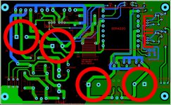
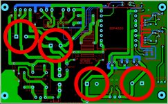
- Fuse is better placed before anything else.
- S1 shorts common mode filter, what is the purpose of this switch?
- J1 tracks are intended to carry 2x the 230V current but are 50% the width. I'm sure there is a better layout for this.
- Could swap R12... and R16 in location for narrower current loop, also swapping AC terminals of diode bridge and maybe more stuff.
- C11 is not needed, but a 390V big MOV at this location is better idea, or for 120V support 2x 200V MOV, one across each 200V electrolytic.
- C8 and C9 are better implemented as a single cap connected to pin 1 of EMI filter.
- C10 is better implemented across transformer, from mains live ground to output ground.
- There is another capacitor missing from output ground to chassis ground.
- C7 can be bigger.
- Optocoupler trace so close to switching pins in transformer is asking for trouble.
- Power layout is bad as hell 1: just connect one end of the transformer to ground, the other end to the inductor, then to the capacitor (a single one is OK), then to switching node.
- Power layout is bad as hell 2: connect the rightmost pin of daugther board right to the FET source terminal with separate PCB track.
- Power layout is bad as hell 3: move feedback stuff to right side of daughter card header.
- Power layout is bad as hell 4: separate the 2 pins that drive high side FET from the other 4 pins that drive low side FET and feedback.
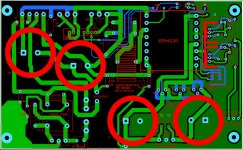
Last edited:
S1 is on-off switch and layout has been corrected, also X1 cap c7,c11 15mm footprint,275VAC if you use 20mm then make this change in your layout, again follow the suggestions of EVA. the MOV will be in final pcb. As for the resonant tank I am not a big fan of the capacitor connected to the switching node, grounding the transformer ,connecting the caps across the fets offers protection and lowers peak current. I will change the daughter pcb to reflect the changes Eva suggest, makes sense. Again this is pcb is to be used as a test bed for me, the final product will have some changes I am sure...
Last edited:
Eva was kind enough to suggest major changes to PCB, so please disregard PCB layout and I will post one to include all her changes and maybe with her help we will end up with a excellent pcb layout.
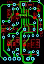
A PCB WITH SOME CHANGES AND THE DAUGHTER
I have made some changes to the earlier pcb and uploading the daughter pcb
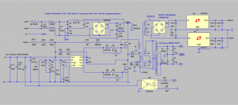
note TH components used because some components will be changed as the board is adjusted to work with main pcb. The appnote AN1160 needs be used with this project it explains a complete design of an IRS27951 converter as well as the calculations needed.
After confirming the design I will be using smd components for the daughter pcb and I will also post it shortly, it follows the appnote schematic .
I have made some changes to the earlier pcb and uploading the daughter pcb
note TH components used because some components will be changed as the board is adjusted to work with main pcb. The appnote AN1160 needs be used with this project it explains a complete design of an IRS27951 converter as well as the calculations needed.
After confirming the design I will be using smd components for the daughter pcb and I will also post it shortly, it follows the appnote schematic .
Attachments
- S1 is connecting input mains to diode bridge skipping EMI filter.
- NTC is skipped when J1 is closed
- MOV has no function as it was placed, needs one 200V MOV for each cap.
- Current C10 location could cause trouble with heatsink. Traces for parts such as C10 should be short, this cap suppresses common-mode EMI of the transformer.
- C9/C55 redundant/wrong, it seems you have trouble understanding EMI filter.
- R16 function can typically be performed by R12...
- More, but too tired to describe until tomorrow.
Last edited:
Maybe, but EMI filtering is a black art and that is why on some appnotes you will find some components for emi filters marked NU (not used)because the spectrum analysis indicated the frequency band was outside design goals, this can only be determined through breadboarding a design, there always be EMI.
EMI filter topology is fully deterministic, unless for "copiers by the looks", then consider you are doing SMPS and this is dangerous. Y caps, X caps, CM chokes, DM chokes if any, bleeder resistor, no more cases. In this case (LLC) it can be reduced to one X cap, one Y cap from one side of X cap to chassis ground, bleeder resistor, one Y cap across transformer. This is assuming secondary ground is also coupled or connected to chassis ground (in audio gear it is usually capacitively coupled to prevent ground loops).
There is another feature of last circuit that deserves being discussed: The FETs are feeding square wave into the transformer, this is not optimum for CM EMI, the FETs should fed square wave to inductor, then to transformer/capacitor.
The issue with the resonant film caps is that the half bridge is better implemented with one thru-hole film cap in series between inductor and transformer (more nH inductance), and 1+ ceramic SMD caps (100n+ 500V+) from +HV to GND (fewer nH inductance), this results in minimal spikes above +HV or below GND when switching. The films in the way you laid them out just reduce spikes by 50%, as trace and capacitor inductance is comparable to electrolytics, Chinese inverter clone style. To get minimum trace inductance +HV and GND traces should go together from series 200V bulk caps to the FETs, using opposite sides of PCB, and the SMD decoupling cap(s) should be placed between the FETs. This is same practice as in class D output stages, allows fastest turn off and lowest switching losses.
Last edited:
- Status
- Not open for further replies.
- Home
- Amplifiers
- Power Supplies
- 700 - 800W LLC Converter