fotios said:
Aq
I gave a detailed explanation of my thesis... i think so.
I don't disagree that the EF isolates the LTP from the Cdom of VAS transistor. Simply, in my practical tests proved that the Cob of VAS transistor used, it is the main reason for the Miller pole presented on VAS by itself. If the EF between LTP and VAS was an absolute solution, then the compensation capacitor accross the B-C junction of VAS it is uselless... but the capacitor is still presented.
Regs
Fotios
The Miller cap across VAS is vital going from my experiments.
Without it I got nasty glitches and oscilation.
nigelwright7557 said:
The Miller cap across VAS is vital going from my experiments.
Without it I got nasty glitches and oscilation.
Right
You have the same experience as me. The issue is that; If we use a transistor with small Cob, then the compensation capacitor will be small to absorb the overshoot and ringing of VAS caused from its Miller capacitance, consequently a higher slew rate can be achived. On the contrary, if the transistor has big Cob then the capacitor will be bigger to compensate, thus causing a lower slew rate.
The higher the slew rate, the better the response in high frequencies
Regs
Fotios
fotios said:
Right
You have the same experience as me. The issue is that; If we use a transistor with small Cob, then the compensation capacitor will be small to absorb the overshoot and ringing of VAS caused from its Miller capacitance, consequently a higher slew rate can be achived. On the contrary, if the transistor has big Cob then the capacitor will be bigger to compensate, thus causing a lower slew rate.
Regs
Fotios
Yes, thats what I found.
Small cap led to glitches and oscilation and too big a cap lost bandwidth.
I think I settled for 220pF in the end.
With other words, the compensation capacitor accross the VAS it puts a limit in high frequencies response (is this which called usually slew limit?) which is the point where the overshoot disappears, consequently the Miller capacitance has compensated.
From my experiments, the RC network accross the main feedback resistor, it can do the same work. We can play with different values in Cdom and in this RC network alternativelly, and maybe we can obtain a better result in high frequencies response (or some higher slew rate).
As for me, i said many times that i use my scope and a square wave generator to measure the rise time of output signal for making my estimations. I find the practical measurement of slew rate very difficult with the few tools that i have.
Regs
Fotios
fotios said:With other words, the compensation capacitor accross the VAS it puts a limit in high frequencies response (is this which called usually slew limit?) which is the point where the overshoot disappears, consequently the Miller capacitance has compensated.
From my experiments, the RC network accross the main feedback resistor, it can do the same work. We can play with different values in Cdom and in this RC network alternativelly, and maybe we can obtain a better result in high frequencies response (or some higher slew rate).
As for me, i said many times that i use my scope and a square wave generator to measure the rise time of output signal for making my estimations. I find the practical measurement of slew rate very difficult with the few tools that i have.
Regs
Fotios
I suspect what is happening is there is a very small delay around the feedback loop which means the output overshoots before the feedback can kick in and reduce the output again.
nigelwright7557 said:
I suspect what is happening is there is a very small delay around the feedback loop which means the output overshoots before the feedback can kick in and reduce the output again.
Yes, i think what you said is the most probable explanation for this interaction between these two different networks, placed in different points in the amplifier circuit.
In ordinary amplifier circuits, there are 3 main points for clamping the upper frequencies:
1. The LTP input filter
2. The Miller compensation capacitor
3. The RC network across the feedback resistor
Between these maybe we can count also the zobel network, because in high frequencies, the resistor becomes very hot which means a significant current flow from output to ground node.
One question: Can we suppose the Miller capacitor as a nested feedback loop inside the main feedback loop?
Regs
Fotios
fotios said:
One question: Can we suppose the Miller capacitor as a nested feedback loop inside the main feedback loop?
Regs
Fotios
I would think so.
Its just slowing down the rate of change around the amp.
It reminds me a bit of servo systems where the gain around the loop has a critical setting to stop overshoot and undershoot.
They call it critical damping....
nigelwright7557 said:
I would think so.
Its just slowing down the rate of change around the amp.
It reminds me a bit of servo systems where the gain around the loop has a critical setting to stop overshoot and undershoot.
They call it critical damping....
Thanks Nigel for the constructive and pleasant discussion.
Here it is 1:25 A.M., time for sleep.
We talk again.
Good night
Fotios
fotios said:
One question: Can we suppose the Miller capacitor as a nested feedback loop inside the main feedback loop?
Yes!
One nice thing about this kind of compensation is that it makes the output impedance of the VAS low at high frequencies making distortion from current drawn by the next stage lower even before global feedback is applied. If the transistor (or darlington combination) has high beta and low capacitance too then it will be very linear too. The nonlinear capacitance of the transistor will be swamped by the capacitor
Also, it gives the front end a very defined transfer function for frequencies above a couple of tens of Hz or so and up to frequencies well above the unity gain crossover of the loop. Vout = (Gm/Cdom) * Integral(Vin*dt) if I'm awake enough

Douglas Self's book has a very good explanation of the nice things about using a miller cap on the VAS for compensation.
The capacitor or RC in parallell with the feedback resistor should be designed to give some phase lead at the unity gain crossover frequency. Observe that making the cap too big will make the amp unstable as gain also increases at the crossover then!
raitraak said:Hey!
Little bump🙂
G.Kleinschmidt, fotios - care to reply to AndrewT?
Regards,
Aq
Well why ask the VAS buffer EF to drive a 50W/8A transistor that will never perform particularly well as a VAS, especially when there are so many much more suitable devices to choose from?
MJE150XX is overkill and sub-optimal for the VAS CCS too.
Cheers,
Glen
by GK - Well why ask the VAS buffer EF to drive a 50W/8A transistor that will never perform particularly well as a VAS
Mjl15032/32 are absolutely unsuitable as a VAS...
SLooow
 , mjl340/350 with the EF is acceptable,
If I were designing this (which I will soon,as I need a sub amp)
I'd use 2sa1381/3503 with optional EF running at 5-7ma,they
have a Cob of 2.3 and allow for a good running/cool/fast VAS
at 47pf Cdom. get the F gain group.
I run a similar LTP/CM and with these 100ma devices I
had to degenerate the VAS/LTP (to much gain). With
that triple EF OP I see, a 5ma VAS would see almost no load.
OS
Hey!
Happy New Year!🙂
Thanks everybody for the replies.
I have substituted MJE340/350 for VAS and also for input current source.
I also have drawn the boards:
MAIN: Schematics Board
MAINPWR: Schematics Board
SOFT_START: Schematics Board
DUAL_PROT: Schematics Board
PREAMP: Schematics Board
PREPWR: Schematics Board
I have to draw one digital board for other project, then i can start making the PCB-s.
Regards,
Aq
Hi raitraak and happy new year
Don't trust Toshibas for VAS and CCS of VAS... with so high voltage rails, they exceed their SOAR... for 15 to 20mA current which needed with simple LTP in input.
Of course MJE340-350, are a better solution. You can feel safe that they dont exceed their SOAR.
There is another one option (the most suitable) if you are disposed to spend about 30euros. The MPSU10-60 of motorola, which are obsolette from OnSemi. But they offered from some online stores in relativelly high price. Check in the web and you will find the obsolette parts in some UK shops.
For the record:
MPSU10-60 => Vce=300V, Ic=0,5A, Hfe=130, Cob=3pF
Unfortunatelly i have spend all of my stock, unless i had send you 2 pairs for free.
This pair used from Peavey in all of its models.
Regs
Fotios
Hey!
Thanks Fotios for the reply! I think I'll stick with the MJE-s for now. Components have been quite expensive.
Does anybody has comments on the PCB-s?
Regards,
Aq
Thanks Fotios for the reply! I think I'll stick with the MJE-s for now. Components have been quite expensive.
Does anybody has comments on the PCB-s?
Regards,
Aq
raitraak said:Hey!
Thanks Fotios for the reply! I think I'll stick with the MJE-s for now. Components have been quite expensive.
Does anybody has comments on the PCB-s?
Regards,
Aq
You can use also BF460 - BF463. Those are same in performance like MPS-Us, and cheaper. Check price here:
http://www.littlediode.com/components/home.php
This store is located in UK
Attachments
jacco vermeulen said:
Plenty others
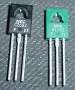
Hmmm....
Those devices in photo, seems to be original NEC parts. I have seen some others fake.
Hi Raitraak,
Very nice amp. Did you simulate it in SPICE?
I have two remarks to the PCBs:
1. On the power amp board (and possibly all the others) the pads for transistors are too small. It will be difficult to solder them (or to desolder, if needed).
2. On the preamp power supply board it seems that the layout for LM317 is incorrect. Shouldn't the pins be in line?
EDIT: what about a trimmer to set DC offset on the output? I've seen similar amps with 300mV on the output.
Mark
Hey!
Thanks everybody!
I received the MJE-s yesterday, and I'll be sticking with them. If they will perform badly, i'll make a switch.
Markus2006:
No, I haven't simulated the schematics, but the design is widespread, so it should work.
I didn't want to make the clearances small, so I decreased the pads, but too much🙂 Clearance is much more than enough. Increased the pads.
The pins should be inline, but I chose to bend them, that makes lot of room. The same with MBR40250 diodes.
I also added the trimmer, just in case🙂
Aq
Hello!
It's been a long time now since any update, but there hasn't been much to report. I have made the boards and assembled them. And then came the problems, of which the biggest one is oscillation of the amp. I've tried to deal with the problem in several ways (removing/replacing/adding components, simplifing the schematics), but nothing hasn't really been working.
Power
Amp
Now to the problem:
The main board:
Schematics
Board
(This is not the latest version, but the changes are minor. I was not able to get PADS working on my Win 7 64 to create the final one).
Now i have reduced the actual schematics to this:
Schematics
But it still oscillates:
Schematics
(CH1, ~10 MHz, 4 Vpp)
When i touch the heat sink, then the oscillation changes.
Schematics
Heat sink is not conncted in any way so this is some capacitive effect. Is it possible the problem lies only in pcb design or is the schematics causing the instability. Could the LONG feedback track cause the problem? Can anyone comment the pcb design?
Without a clue🙂,
Rait
- Status
- Not open for further replies.
- Home
- Amplifiers
- Solid State
- 300 Watt Amp