Precarious tantalum application
Andrew, there are four each 330uf totals 1500uf combined as an array, but isn't 330*4 =1320?
Anyhow, since unconfirmed voltage rating, conservative approach is to assume voltage rating below 7809 powering, so substitute a lower dc voltage, check current legitimacy since quiescent consumption of current is a couple milliamps. Fuse the current specified for normal little gem mark II consumption. Should the tantalum array blow, it will be a big short. I benched it out of circuit by charging it to multimeter battery voltage applied during capacitance measurement, some mere fractional volt, but it stubbornly retains charge, meaning good zero leaks. Thats why must chk next charge to six dc volts, simple 6v lantern battery charge up endure, then if ok, apply nine volts powering. I'll picture post so size is revealed of built array, like the size of my galaxy sIII keyboard button size, held horizontally viewed.
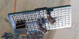
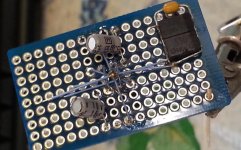
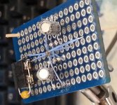
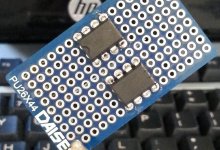
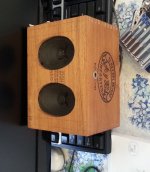
pics little gem substrate
pics of tantalum bank supporting little gem mark II, but buffer portion not appended just yet to substrate, must test gem's tantalum bank ability to accept voltage targeted 9vdc regulated
pics of tantalum bank supporting little gem mark II, but buffer portion not appended just yet to substrate, must test gem's tantalum bank ability to accept voltage targeted 9vdc regulated
Attachments
The little gem mark II web schematic class "B" reveals different versions you can utilize of LM386N-1, 2, 3, 4
I chose whatever bankrupt radioshack sold me, quarter per piece!
The perforated welled landings substrate is humbug dealing with, I'd rather freespace weld the gem package as was done its ahead upstrm buffer weld package.
pcb evolution must be made easier, as in hand drawn conductor traces and hand penetrating landing wells. Nothing much has improved since I was a kid taking electronics in public education. That was the vietnam war back in the 60's!
Do you visual the kynar segmented congestion of conductor routing on this humbug substrate? Thatts humbug fabrication! Intent of layered planes of kynar linkups is to minimize crosstalk and noise intrusion. kynar segmented planes of links esp thwarting competitive earthing amongst energy consumption routes. Laid earth linkages of kynar on ground floor substrate, then elevated yea millimeter skywards another kynar conductor path distributing user signal, and finally on the 3rd floor yea millimeter higher upwards is the consumption powering tension.
It's trauma to work backwards de-constructing welds to swap out discrete participants!
That means non conducive perfecting optimal circuitry arrangements because of the hassles to remove reinstall access interferences! Kinda reminds me of "building a ship in a bottle". Same thing of obstructions to access are encountered in extremely compacted engineering designs, like our subs, missles, recon satellites, now drone and fugure nano drone! I guess you pay painfully for specialized constructed packages, coveted packages.
Luckily I caught the under rated voltage of tension ballast array comprised of four rectanguloid smd chip tantalums. I detached the positive tension bussing, then independently battery charged this bank to various battery voltages avail, 1st 3v, 2nd 6v, last 9v. Ammeter reveals flow once charge saturated into bank, but current still weeps thru to upkeep battery voltage to par, so that flow is parasitic because its telling you your bank has annihilation going on inside, so scrap it, get a better bank. The bank of four each chip tantalums will be removed from substrate and another electrolytic installed instead with 104bypass as is requested for speedy bypassing. I located a japanese 10v 105celcius brown cylinder radial electrolytic 500uf and its just about the same volume as the bank array tantalums. I realized it's an aluminum electrolytic but it does not suck amperes from battery testing upon complete charge up (instantaneous practically speaking). Other electrolytics maintain steady ampere (ma) draw even after chargeup. So the better the nonleakage (annihilation of energy stored inside electrolytic), the better the cap. But I don't know how conductive performance will be, as caps do exhibit sluggishness transacting charge balance negotiation to demands. I pay attention here because response time affects guitar outcome sound signatures. Materials used to construct caps exhibit real world characteristics! Its not perfection so cap will not follow ideal laws of capacitance, it has compromising influence, from resistivity, inductance, probably more influence from range of frequencies passed, and atmospheric meteorological conditions affect too. All that said of the condenser ballast for tension desired. Looks like tension will always be behind schedule! The vacuum tube folks some adore "sag" inherent to tube rectifier bottle. And that's coupled to condenser bank itself always behind schedule to guitarist demands of promptness, and so the coveted gube rectifier.
new concern, the substrate indicator light, old fashion red led sized BB shot still drinks 4.84ma 1.75vdc drop seried to eighth watt 1k5 resistor placed across regulator 7809 output 9vdc. too much milliampere. concern is drawing current unnecessarily, why, loading upreach powering supply which is legacy japan 9vdc unregulated transformer fullwave rectified and smoothed feeding 7809 package positioned afar from xfmr by orig japan cabling furnished w/ xfmr (must be kinda ancient "PA7482U"). 7809 still works flawlessly because the xfmr package puts out beyond 9vdc (freewheel is 12plus vdc). the concerned red LED package is to be welded to the gem substrate ballast 500uf by 10wvdc locally. that means quiescent totalized current is roughly 3ma for buffer, 5ma red led, 30plus ma Gem package. now what happens during guitar signal processing demanded?does current remain identical to quiescent status or does it escalate according to guitar signal processing demands? i always thought audio class A signal amplification processing burns the same amount of fuel regardless of guitarist signal processing demands. clarification? i can still resort to modern green ultrabright micro LED and run it at fractional milliamperes thru 10^4 resistor across 9vdc. so LED loading can significantly be reduced if need be. so this post on clarification. maybe it is perfectly alright to load 5ma LED, why, current preloading that prehistoric japan xfmr places xfmr into operational regime to better transfer (induct), kinda analogous to tweaking the karmin ghia carburetor idling screw to set rpm quiescent.
Is that spkr parallel zobel r-c required?
web literature says its needed to absorb bounce aberration of the impefect spkr 's mechanicals tracking power amplifier drive. others say no need zobel when spkr proper impedance for power amp and spkr wire short, how short, how matched impedance?
maybe use zobel with seried potentiometer to cut it in slowly and examine behavior?
anyone tried short leads and matched impedance?
8 ohm spkr fed dc from pin 5 and pin 5 of dual LM386N-1
anyone know if i gotta series wire in an electrolytic cap for spkr connections?
i'm getting about 3vdc! positive observing 386/spkr polarity connection by runoff groove's little gem mark II circuit shown. that circuit does not put a dc blocking series connected electrolytic at all, and if you need it, do you need two each since two each LM386N-1 ?
ammeter powersupply revealed couple tenths of full ampere! that's excessive, why, current should ball park to one watt thereabouts (9vdc) * (1/9)ampere=1watt
one ninth ampere is roughly 100ma
i checked my physical project for shorts, there are none.
correctness of circuitry is fine.
so, what?, maybe buffer feeding pure dc into power amp?
gotta chk dwnstrm jfet's dc blocking cap output for any presence voltage dc passage?
but wait, this node is directly connected to opposing phase inputs into the dual 386 amps. unused 386 input nodes are earthed.
if buffer feeds dc dwnstrm, it means it's exiting dc blocking cap is bad. if it is good, then where does spkr's dc problem come from? bad 386 chip? maybe, yikes, reversal of welds to swap out 386 chip is nightmare
any other possibilities why spkr dc has resulted?
i can subst a resistor for spkr but am uncertain whether some weakest link will blow since 386amp not made to pass dc to spkr nor drink so much fractional amperes. prolonging energization to take more measurements may blow the weakest link and or culprit yet found. don't want to blow vc of paper spkr taken from ancient japan boombox portable player (good span of sounding for 3" dia 8ohm 1.5w)
culprit found and cleared, amber residue bridging
i found the bug. it is that china amber stuff called amtech flux rma-223-uv "made in usa!"
pure isopropanol and tiny paint brush bristle agitation submerged workpiece washed all cross connects bridged by amber deposits
fired it up with spkr, quiescence measures 48ma by 256mvdc positive across spkr
but 256mv is unacceptable so what do?
china schematic shows bridged mode pair 386 with their pin sevens cross connected by a half meg pot, maybe for zero'ing this 256mv dc across spkr?
anybody knows why such 386 chip pin seven bridging with pot is used?
Low Voltage Bridge Audio Amplifier - Amplifier Circuit Design
but the 10uf pin 1&8 differs
and the 500k pot is not across both pin 7's
i could have sworn someone already referred this circuit showing pin 7's used for the 500k pot adjust
but the 10uf pin 1&8 differs
and the 500k pot is not across both pin 7's
i could have sworn someone already referred this circuit showing pin 7's used for the 500k pot adjust
Low Voltage Bridge Audio Amplifier - Amplifier Circuit Design
but pin 7's not the 500k pot adjust, so could i have got the wrong diagram here?
somebody posted the picture of same and it had a chinese logo bottom right hand of pic, i swear the pin 7's were used for the 500k pot
but pin 7's not the 500k pot adjust, so could i have got the wrong diagram here?
somebody posted the picture of same and it had a chinese logo bottom right hand of pic, i swear the pin 7's were used for the 500k pot
- Status
- Not open for further replies.
- Home
- Live Sound
- Instruments and Amps
- 2SK170GR buffer guitar