At the risk of being in the gunsight of the moderator, let me clarify my stand.
I had built the JLH with TO-3 devices long back and had assiduously followed the diyaudio thread.
I have been a fan of Mr Juma's simple and rewarding designs for long.
I had got together all the stuff for building the #1 post design, when he posted the new variant in # 180.
I thought if Mr Juma would be kind enough to offer a similar topology for the #1 circuit, I could build one of each and try listening over a period, before deciding on the final configuration.
It is as simple as that.
It was this urgency on my part (and also Mr Juma's professed dislike for using PM to clarify doubts) that spawned a series of questions.
I am sure many, including Mr Juma and Mr Pass, would appreciate this, and not view it as mere nitpicking from an idler.
I am sorry if I have upset the mood of the thread.
Warm regards, as always.
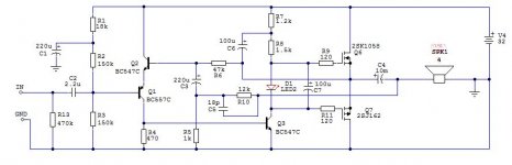
Could you please tell, what is the role of transistor Q3?Hi Skorpio,
I tested your 2-loops idea and it brings some improvement indeed
I also changed the input device into N-JFET which made some other changes necessary and the whole thing now looks like this (and sounds somewhat better) 🙂
Please don't ask me about parts substitutes, power increase or to compare it with other amps/designs....
The input FET Q1 has already have a cascode Q2. Seems like Q3 is taking the feedback current as input and giving its output to FET Q1, but not very clear what is the function of Q3 here.
I have the same question as sarathssca. I've been tinkering with similar JFET singleton IPS designs in LTSpice and this transistor seems to help. But it's not clear to me why. Is it buffering the current feedback to Q1?
Q3 is a part of so called Rush cascode, together with Q1. Its base is a feedback node transfered via Q3's emitter to Q1's source - similar to mechanism more often seen in LTP.
Q2 is a standard cascode and besides linearisation of the input stage it has a task to provide low Vds for Q1 in order to avoid gate leakage in Q1 so we can have high Zin (R2 || R1).
You can read more about Rush cascode elsewhere - there are numerous threads about it on this forum too.
Maybe it is clearer if drawn this way (BJT PNP input, "normal polarity" PSU).
Attachments
Last edited:
Maybe it is clearer if drawn this way (BJT PNP input, "normal polarity" PSU).
I like this, looks a bit like the old NAD3020 phono stage 🙂
But I also like the low impedance feedback point of the original design, so I will try not to modify 😀
Hi Skorpio
it is an intermediate version, post #180 shows what I liked better.
Anyway, the differences are not big, you enjoy what you like
it is an intermediate version, post #180 shows what I liked better.
Anyway, the differences are not big, you enjoy what you like
The Rush cascode converts the input stage to an ugly differential amplifier. Gate leakage is not reduced, nothing is linearized, instead instability and high distortion introduced. The topology using two single ended stages is realizable without any capacitors, other than an output capacitor.
Last edited:
@ Juma:
Sir, is post #224 a re-drawn circuit (simmed?) for explaining the concept, or is it 'buildable' as such?
Thanks and regards.
Sir, is post #224 a re-drawn circuit (simmed?) for explaining the concept, or is it 'buildable' as such?
Thanks and regards.
Yes Prof, I built it. Only variable is R1 - you can vary it to get half of the PS voltage on sources of MOSFETs.
juma,
you have made improvements on the original design, but the differential amplifier is not a qualitative progress.
you have made improvements on the original design, but the differential amplifier is not a qualitative progress.
@ Juma:
...in that case I shall build that instead of Post #1 ... go with the latest!
;-)
Warm regards.
...in that case I shall build that instead of Post #1 ... go with the latest!
;-)
Warm regards.
...certainly, for one channel -- with your twin loop feedback, now approved by the master himself!
The second channel will be # 224.
Quick march...and keep the ears cleaned !
The second channel will be # 224.
Quick march...and keep the ears cleaned !
Hi Skorpio,
I tested your 2-loops idea and it brings some improvement indeed
I also changed the input device into N-JFET which made some other changes necessary and the whole thing now looks like this (and sounds somewhat better) 🙂
Please don't ask me about parts substitutes, power increase or to compare it with other amps/designs....
If I wanted to tune down the gain in this circuit would I increase R8 or decrease R9? I am looking for something like 14V/V.
I presume R10=100k is the smallest you can get away with to have enough base current for Q3 so better not touch it?
I don't get how R11/R12 work. Would they need to be adjusted for different gain?
use R9 to adjust gain.
leave R10 alone, it defines DC conditions too.
R11, R12, C5 are bootstrap load for Q4.
leave R10 alone, it defines DC conditions too.
R11, R12, C5 are bootstrap load for Q4.
Thx, understood.
Can you shed some light how you dimensioned R11, R12?
I understand that the sum sets the collector current of Q4.
Other references I found split the total collector resistance evenly to attach the bootstrap capacitor. You use different values, is there something to learn from this?
Can you shed some light how you dimensioned R11, R12?
I understand that the sum sets the collector current of Q4.
Other references I found split the total collector resistance evenly to attach the bootstrap capacitor. You use different values, is there something to learn from this?
- Home
- Amplifiers
- Pass Labs
- 25W Class A amp with Lateral MOSFETs