Lessons learned from preceding designed, I understood that it is unrealistic to seek distortions bellow 0.0001% at 10khz 30Vp, where noise dominates the measurements.
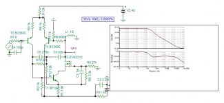
Instead of designing the IPS and VAS separately , Why not design them together . As my OS has a distortion 0.0013% for 30Vp 10khz , with hybrid version it showed that 30db NFB is sufficient. To have an overall gain of 25db, only 55db is necessary for the (IP+Va) stage to provide.
The circuit bellow has a distortion of 0.0005% , with mosfet inputs zvp3310 it is slightly lower, Jfets also can be tried out.

Hayk
Instead of designing the IPS and VAS separately , Why not design them together . As my OS has a distortion 0.0013% for 30Vp 10khz , with hybrid version it showed that 30db NFB is sufficient. To have an overall gain of 25db, only 55db is necessary for the (IP+Va) stage to provide.
The circuit bellow has a distortion of 0.0005% , with mosfet inputs zvp3310 it is slightly lower, Jfets also can be tried out.
Hayk
Attachments
Last edited:
In the diagram, the inductance L1 is connected to the ground, and not to the plus?
Is it a correction element or a cascade load?
Is it a correction element or a cascade load?