After a limited succes with the previous 0-15V 72A prototype, I'm working on this new one.
The old prototype was based on a PWM full bridge with synchronous rectification and worked fine as long as voltage control was used. However, I got a lot of trouble when I tried to implement average current control, mostly due to transformer saturation and probably also related to a lack of symmetry between secondary windings. Anyway, PWM full or half bridges with the buck inductor in the secondary side doesn't cope well with the quick duty cycle changes required for proper transient response.
I could have used peak current control, but it doesn't suit my needs. I need average current control because I want to connect several PSUs in paralell and obtain perfect current sharing by just ORing the current command buses (the one with the highest voltage preset will drive the rest).
That is why I'm about to try a different topology with the buck inductor in the primary side. It looks like a standard buck converter with a switch, an inductor and a diode in the primary side, but the output capacitors are placed on the secondary side and are transformer coupled. In this topology the transformer is always operated at 100% duty cycle and there is an inductor in series with it, so flux balance is guaranteed (I think...).
I've tried that topology in the past with succes, but I couldn't make PCBs at that time so the prototype was a mess of wires. Furthermore, I was using hard switching so there were lots of EMI and ringing. I was not able to improve EMI, so I abandoned the project.
The full bridge is essentially the same I was using in the previous prototype. Switching devices are MJE13009 bipolar transistors with proportional base drive.
I'm also going to try a magnetic snubber approach to achieve soft switching in continuous conduction mode. It works fine in the 2KW PFC prototype so it should also work fine here. L2 from the PCB is the center-tapped inductor that limits dI/dt.
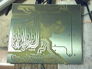
This is the layout of the primary-side prototype PCB, IC1 is a CD4013 flip-flop for bridge sequencing and IC2 is a CD4049 hex inverting buffer, I will etch the PCB soon:
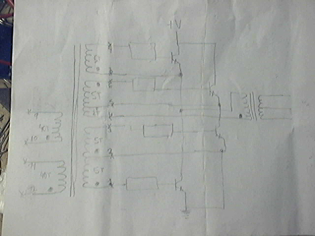
And this is a simplified schematic, don't trust all component values and note that the CMOS ICs are missing:
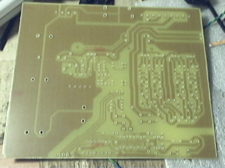
The secondary-side synchronous rectification PCB is already finished. This is the layout:
http://eva.eslamejor.com/100a_1.gif
And some pictures:
http://eva.eslamejor.com/100a_1_0.jpg
http://eva.eslamejor.com/100a_1_1.jpg
http://eva.eslamejor.com/100a_1_2.jpg
http://eva.eslamejor.com/100a_1_3.jpg
http://eva.eslamejor.com/100a_1_4.jpg
http://eva.eslamejor.com/100a_1_5.jpg
http://eva.eslamejor.com/100a_1_6.jpg
The rest of the stuff (SG3525 control IC, current and voltage amplifiers, etc..) is in bread boards so I can play freely with it.
I hope this could be useful for other people trying to design their own SMPS stuff.
The old prototype was based on a PWM full bridge with synchronous rectification and worked fine as long as voltage control was used. However, I got a lot of trouble when I tried to implement average current control, mostly due to transformer saturation and probably also related to a lack of symmetry between secondary windings. Anyway, PWM full or half bridges with the buck inductor in the secondary side doesn't cope well with the quick duty cycle changes required for proper transient response.
I could have used peak current control, but it doesn't suit my needs. I need average current control because I want to connect several PSUs in paralell and obtain perfect current sharing by just ORing the current command buses (the one with the highest voltage preset will drive the rest).
That is why I'm about to try a different topology with the buck inductor in the primary side. It looks like a standard buck converter with a switch, an inductor and a diode in the primary side, but the output capacitors are placed on the secondary side and are transformer coupled. In this topology the transformer is always operated at 100% duty cycle and there is an inductor in series with it, so flux balance is guaranteed (I think...).
I've tried that topology in the past with succes, but I couldn't make PCBs at that time so the prototype was a mess of wires. Furthermore, I was using hard switching so there were lots of EMI and ringing. I was not able to improve EMI, so I abandoned the project.
The full bridge is essentially the same I was using in the previous prototype. Switching devices are MJE13009 bipolar transistors with proportional base drive.
I'm also going to try a magnetic snubber approach to achieve soft switching in continuous conduction mode. It works fine in the 2KW PFC prototype so it should also work fine here. L2 from the PCB is the center-tapped inductor that limits dI/dt.
This is the layout of the primary-side prototype PCB, IC1 is a CD4013 flip-flop for bridge sequencing and IC2 is a CD4049 hex inverting buffer, I will etch the PCB soon:
An externally hosted image should be here but it was not working when we last tested it.
And this is a simplified schematic, don't trust all component values and note that the CMOS ICs are missing:
An externally hosted image should be here but it was not working when we last tested it.
The secondary-side synchronous rectification PCB is already finished. This is the layout:
http://eva.eslamejor.com/100a_1.gif
And some pictures:
http://eva.eslamejor.com/100a_1_0.jpg
http://eva.eslamejor.com/100a_1_1.jpg
http://eva.eslamejor.com/100a_1_2.jpg
http://eva.eslamejor.com/100a_1_3.jpg
http://eva.eslamejor.com/100a_1_4.jpg
http://eva.eslamejor.com/100a_1_5.jpg
http://eva.eslamejor.com/100a_1_6.jpg
The rest of the stuff (SG3525 control IC, current and voltage amplifiers, etc..) is in bread boards so I can play freely with it.
I hope this could be useful for other people trying to design their own SMPS stuff.
looks nice!
I am bit supprised how much power you can beat out of mj15003, 1.8kW with four to-220 bipolar transistors. I guess that enough low frequency and proper base drive does the trick.
What kind of like transformer structure you are using?
I am bit supprised how much power you can beat out of mj15003, 1.8kW with four to-220 bipolar transistors. I guess that enough low frequency and proper base drive does the trick.
What kind of like transformer structure you are using?
Well, I think i've got it to work fine (or something like that). The funniest part is that I solved the asymmetry issue in the old prototype the same day I etched the new buck+bridge board, and I couldn't resist to try the new 120A synchronous rectification board in the old bridge prototype since it was ready to use and I felt too lazy to start populating the new PCB.
The asymmetry issue was related to several flaws. First, each of the push-pull secondaries is in an independent layer so its DC resistance and leakage inductance are not exactly the same. Second, in the base drive transformer, the leakage inductance from the two-turn current-sense winding to each base-drive winding depends on how these two turns are placed, so misplacement causes a slightly amount of asymmetric base drive. Third, the output signal of the voltage amplifier was picking up asymmetric noise at the switching frequency before it was fed to the input of the current amplifier, so I had to low-pass filter it.
Fourth and most important, the current sense transformer was failing to sense DC or LF errors introduced by the three previous flaws, it was saturating badly instead, thus causing even more asymmetry. I solved that last issue by operating the current-sense transformer in a nearly zero-flux fashion, this was achieved by loading it with cascode transistors thus not allowing it to see the voltage drop across the load resistor. Now it can measure very low frequencies approaching DC and this is enough in order to allow the current amplifier to correct potential flux asymmetries in main transformer.
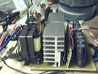
Some pictures:
This is the finished buck+bridge board. I have obviously found a way to continue using the old topology with success, and it is much simpler and cheaper, so I think I'm going to discard the new topology for that project. Anyway, I think I have already found another use for it: 1800W regulated audio amplifier PSU with multiple tightly coupled outputs but without messing with multiple buck inductors. This topology is very convenient for that purpose.
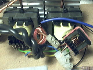
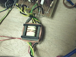
These two are the main transformers placed on the new 120A synchronous rectification board. Cores are E42/21/20 of unknown material, most likely N27 or similar. Primary is split in two layers connected in series and secondaries are sandwitched between them. Each push-pull secondary winding consists of a single layer made with 4 turns of 1mm wire. Each secondary layer is made with 12 turns of twin 0.75mm wire. All four primaries are connected in series so perfect current sharing is guaranteed. The picture also shows the 100:1 current sense transformer, and an additional 5uH inductor connected in series with the primaries in order to limit dI/dt.
This picture shows the buck inductor, it's made with E42/21/20 cores and 3.2mm gap on all legs (6.4mm total). It is wound with 7 turns of ten 1mm wires. It keeps approx. 5uH inductance up to 100A, then it starts progressively saturating but it's still usable up to 120..130A. I feel that copper losses at 120A may be too high so I may end up using two paralell. inductors instead.
This is another picture of the synchronous rectificacion board. Note that I have left the wires of both secondary windigns with the same lenght and I have bent the remainder in an attempt to improve symmetry.
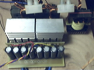
Another view of synchronous rectification board, this clearly shows the remainder of wire of the inner and shorter secondary winding bent.
This is the bottom side of the synchronous rectification board. The output is taken from these pairs of black and blue 6mm^2 wires. Blue is ground. This picture also shows series connection of primary windings.
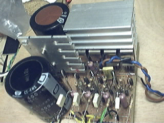
This is the venerable MJE13009 full-bridge board. It has survived lots of modifications and several catastrophic failures in the past two years, so it's a bit messy and some components look a bit darkened due to others exploding . However, I have not blown any MJE13009 for the past six moths or so. Anyway, I'll have to upgrade it since two 470uF capacitors are not enough to get reasonable ripple with 1800W load, four capacitors are required.
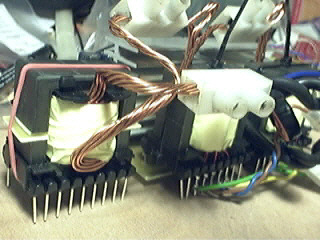
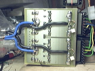
First picture shows the base drive transformer, it's a hell to wind it, look at its layout in second picture. 40T windings are made with two 0,22mm wires, one winding per layer. 5T windings are made with four 0,22mm wires, two windings per layer, and they are sanwithched between the 40T ones.
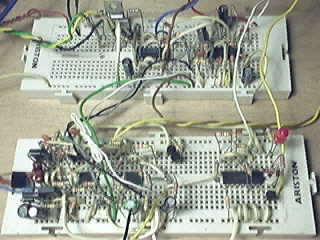
This is the messy control circuit built in bread boards. It contains smart things like inductor current waveform synthesis using the primary side current waveform as a starting point. It also has a potentiometer (not shown) to adjust output current limit between 3A and 120A. The red led lights when synchronous rectification is turned on, it must be current triggered, it can't be turned on all the time in order to avoid catastrophic failures, for example when mains power is cut while a 12V battery is connected to the output (I have experienced this situation with previous prototypes during field testing at car-audio shows and it was quite frustrating). There is also a SG3525 control IC and two HUF75309 MOSFETs that are driven from a CD4049 CMOS inverting buffer and control the turn-off phase of bipolar transistors of the full bridge. It's a pity that the SG3525 output signals have the wrong polarity.
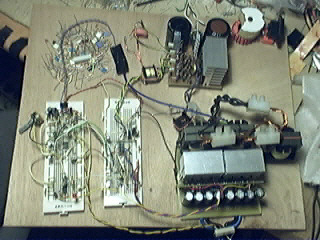
And finally, this shows an overall view of the prototype.
Currently I'm trying to further reduce losses in the full bridge since losses in the synchronous rectifiers are already low, its heatsinks only get warm after several minutes of full-load operation. However, the full-bridge heatsink starts to feel a bit discomfortable to the touch after one minute of operation at full load, it definitely requires a fan to avoid thermal runaway.
I know that the black anodyzed version of these heatsinks features 3.75ºK/W thermal resistance, but I don't know Rth figures for the bare aluminium ones that I have. I want to estimate dissipation figures anyway so I'm planning borrow a temperature probe and do some comparisons against temperature increase figures produced by know dissipations.
I think that less than 40W are lost in the bipolars and approx. 15W + 15W in the rectifiers at full load. I don't think that worst-case losses at full load could be higher that 100W, so efficiency is 95% or greater 😀
I like these bipolar transistors, they feature less than 1.5V voltage drop when saturated, usually 1V, even with 10A Ic. They also feature fast crossover times that get smaller as Ic is increased, approx. 100ns for Ic=5A and 50nS for Ic=10A. The only thing I don't like is additional losses due to excessive voltage drop during the first 500..1000nS of each switching cycle when the device is still saturating, that's why I'm adding a series inductor to reduce dI/dt, it doesn't hurt maximum effective duty cycle too much since operation frequency is now 33Khz.
Now I'll go back to experimentation...
The asymmetry issue was related to several flaws. First, each of the push-pull secondaries is in an independent layer so its DC resistance and leakage inductance are not exactly the same. Second, in the base drive transformer, the leakage inductance from the two-turn current-sense winding to each base-drive winding depends on how these two turns are placed, so misplacement causes a slightly amount of asymmetric base drive. Third, the output signal of the voltage amplifier was picking up asymmetric noise at the switching frequency before it was fed to the input of the current amplifier, so I had to low-pass filter it.
Fourth and most important, the current sense transformer was failing to sense DC or LF errors introduced by the three previous flaws, it was saturating badly instead, thus causing even more asymmetry. I solved that last issue by operating the current-sense transformer in a nearly zero-flux fashion, this was achieved by loading it with cascode transistors thus not allowing it to see the voltage drop across the load resistor. Now it can measure very low frequencies approaching DC and this is enough in order to allow the current amplifier to correct potential flux asymmetries in main transformer.
Some pictures:
This is the finished buck+bridge board. I have obviously found a way to continue using the old topology with success, and it is much simpler and cheaper, so I think I'm going to discard the new topology for that project. Anyway, I think I have already found another use for it: 1800W regulated audio amplifier PSU with multiple tightly coupled outputs but without messing with multiple buck inductors. This topology is very convenient for that purpose.
These two are the main transformers placed on the new 120A synchronous rectification board. Cores are E42/21/20 of unknown material, most likely N27 or similar. Primary is split in two layers connected in series and secondaries are sandwitched between them. Each push-pull secondary winding consists of a single layer made with 4 turns of 1mm wire. Each secondary layer is made with 12 turns of twin 0.75mm wire. All four primaries are connected in series so perfect current sharing is guaranteed. The picture also shows the 100:1 current sense transformer, and an additional 5uH inductor connected in series with the primaries in order to limit dI/dt.
This picture shows the buck inductor, it's made with E42/21/20 cores and 3.2mm gap on all legs (6.4mm total). It is wound with 7 turns of ten 1mm wires. It keeps approx. 5uH inductance up to 100A, then it starts progressively saturating but it's still usable up to 120..130A. I feel that copper losses at 120A may be too high so I may end up using two paralell. inductors instead.
This is another picture of the synchronous rectificacion board. Note that I have left the wires of both secondary windigns with the same lenght and I have bent the remainder in an attempt to improve symmetry.
Another view of synchronous rectification board, this clearly shows the remainder of wire of the inner and shorter secondary winding bent.
This is the bottom side of the synchronous rectification board. The output is taken from these pairs of black and blue 6mm^2 wires. Blue is ground. This picture also shows series connection of primary windings.
This is the venerable MJE13009 full-bridge board. It has survived lots of modifications and several catastrophic failures in the past two years, so it's a bit messy and some components look a bit darkened due to others exploding
. However, I have not blown any MJE13009 for the past six moths or so. Anyway, I'll have to upgrade it since two 470uF capacitors are not enough to get reasonable ripple with 1800W load, four capacitors are required.
First picture shows the base drive transformer, it's a hell to wind it, look at its layout in second picture. 40T windings are made with two 0,22mm wires, one winding per layer. 5T windings are made with four 0,22mm wires, two windings per layer, and they are sanwithched between the 40T ones.
This is the messy control circuit built in bread boards. It contains smart things like inductor current waveform synthesis using the primary side current waveform as a starting point. It also has a potentiometer (not shown) to adjust output current limit between 3A and 120A. The red led lights when synchronous rectification is turned on, it must be current triggered, it can't be turned on all the time in order to avoid catastrophic failures, for example when mains power is cut while a 12V battery is connected to the output (I have experienced this situation with previous prototypes during field testing at car-audio shows and it was quite frustrating). There is also a SG3525 control IC and two HUF75309 MOSFETs that are driven from a CD4049 CMOS inverting buffer and control the turn-off phase of bipolar transistors of the full bridge. It's a pity that the SG3525 output signals have the wrong polarity.
And finally, this shows an overall view of the prototype.
Currently I'm trying to further reduce losses in the full bridge since losses in the synchronous rectifiers are already low, its heatsinks only get warm after several minutes of full-load operation. However, the full-bridge heatsink starts to feel a bit discomfortable to the touch after one minute of operation at full load, it definitely requires a fan to avoid thermal runaway.
I know that the black anodyzed version of these heatsinks features 3.75ºK/W thermal resistance, but I don't know Rth figures for the bare aluminium ones that I have. I want to estimate dissipation figures anyway so I'm planning borrow a temperature probe and do some comparisons against temperature increase figures produced by know dissipations.
I think that less than 40W are lost in the bipolars and approx. 15W + 15W in the rectifiers at full load. I don't think that worst-case losses at full load could be higher that 100W, so efficiency is 95% or greater 😀
I like these bipolar transistors, they feature less than 1.5V voltage drop when saturated, usually 1V, even with 10A Ic. They also feature fast crossover times that get smaller as Ic is increased, approx. 100ns for Ic=5A and 50nS for Ic=10A. The only thing I don't like is additional losses due to excessive voltage drop during the first 500..1000nS of each switching cycle when the device is still saturating, that's why I'm adding a series inductor to reduce dI/dt, it doesn't hurt maximum effective duty cycle too much since operation frequency is now 33Khz.
Now I'll go back to experimentation...
I've been doing further testing at various power levels between 1,000W and 1,800W and I think that there are some sections that will definitely have to be oversized, namely the output inductor (too much I^2*R losses, altough some air flow helps a lot), the mains diode bridge (currently a 6A unit on a small heatsink where you can fry an egg), and the heatsink of the bipolar switching transistors (two units instead of one, since they tend to dissipate as much as both banks of synchronous rectifiers together).
I will also have to oversize my test load, consisting on some recycled copper wire wrapped arround a couple of bricks with forced air cooling, they doesn't cope very well with more than 1KW continuous dissipation (it's a nice electric heater, though).
I will also have to oversize my test load, consisting on some recycled copper wire wrapped arround a couple of bricks with forced air cooling, they doesn't cope very well with more than 1KW continuous dissipation (it's a nice electric heater, though).
That kind of testing is better in the winter!
OK maybe you could make an electric BarBQ!
😀 😀 😉
Mark
OK maybe you could make an electric BarBQ!
😀 😀 😉
Mark
Your project is impressive. For dummy loads, I make them out of steel concrete rebar tie wire. It is cheap and holds up to heat better than copper. One problem is getting a good connection between the copper leads and the steel wire. I wrap about ten turns of copper wire around the steel, then wrap steel around the copper. I used it up to 30 amps. The temperature of the 16awg steel wire didn't go over a few hundred degrees at that current level.
An externally hosted image should be here but it was not working when we last tested it.
This is a 120A load step without any preload (except a 60 ohm permanent dummy load) and with very high di/dt, the load is switched in less than a microsecond by a bank of MOSFETs so load inductance dominates. Red trace shows output voltage at 200mV/div (actually measured with a 100:1 high voltage probe that was placed near the switching stuff at 2mV/div, that's why it's so noisy, I was too lazy to look for the 1:1 probe 😱 ). Blue trace is primary current in 2A/div or secondary current in 24A/div (transformer has 12:1 turn ratio). Time is at 200us/div.
I can 'speed up' the voltage amplifier even further, yielding a smaller dip in otput voltage waveform, but at the expense of noise inmunity. This is the fastest compensation that produces no audible jitter with just the dummy load, however, breadboards are evil, I think that mounting it in a PCB would allow for a 'faster' compensation.
Note that output capacitance is pretty small for such big load steps, there are just eight 2200uF 25V capacitors with 0.022 ohm ESR. This means that the the load step by itself is already causing 330mV or more voltage drop until the buck inductor is charged up to the output current level and balance is restored.
Any thoughts?
Speeding up the compensation as the only measure you take might be more problematic. The complete system wil tend to more instability after a certain point.
Since it is a wide range adjustable SMPS (0-15V), I think a feedback with just one timeconstant will not fit for all the needs. If you use a nested feedback (one fast, one slow time constant), it might be worth to see if things get better during a load change.
hth,
Andreas
Since it is a wide range adjustable SMPS (0-15V), I think a feedback with just one timeconstant will not fit for all the needs. If you use a nested feedback (one fast, one slow time constant), it might be worth to see if things get better during a load change.
hth,
Andreas
tekman said:Speeding up the compensation as the only measure you take might be more problematic. The complete system wil tend to more instability after a certain point.
Since it is a wide range adjustable SMPS (0-15V), I think a feedback with just one timeconstant will not fit for all the needs. If you use a nested feedback (one fast, one slow time constant), it might be worth to see if things get better during a load change.
hth,
Andreas
This is an average-current controlled system. It has a current amplifier that forces inductor average current to track the output of the voltage amplifier up to 10Khz. The optimum gain of this current amplifier is inversely proportional to the output voltage, but adjusting it for 16V output does not mean that dynamics are going to be worse for lower output voltages, it just means that dynamics could be better if maximum output voltage was lower.
Anyway, I'm playing with the voltage amplifier and its compensation is not output-voltage dependent, it only depends on output capacitors. It should have a zero at the resonant frequency of the output filter (approx. 300Hz for that design) and a pole above (Fsw/2*pi) in order to filter switching ripple. The magnitude of the dip during load transients depends on the gain it is allowed to have betweem its zero and its pole. Too much gain causes oscillation between 5Khz and 10Khz due to a lack of phase margin. Too low gain causes a huge dip in output voltage when load is increased.
Today I found out that my previous LM358 voltage op-amp was not up to the job of having more than 30dB of gain at 10Khz with little phase shift, so I tried a better one and it allowed me to double the gain to 36dB without any trace of instability. As a bonus, the dip in output voltage during a full load transient was reduced to approx 100..150mV. I didn't use a better op-amp from the beggining because I always like to get the best possible performance from low-cost components, I hate exotic stuff.
Also, the base drive circuit is somewhat flawed since it provides a negative base current for turn-off that is proportional to the duty cycle. In other words, the circuit won't probaly operate reliably with 120A output at low output voltages, so I'm going to add some degree of foldback curreng limiting below 8V output. Anyway, this PSU is intended for automotive electronics applications so it will be adjusted for 12V or 14.4V most of the time.
Danko said:Eva, where do you get the synchron-signal, to which mosfet turn ON or OFF?
Both push-pull banks are turned on by default, except when estimated inductor current is low (body diodes of MOSFETs are used as plain diodes for low currents). Each positive-going signal from the SG3525 turns off the right bank of MOSFETS just 500ns before the primary full-bridge is switched in that directon. Then, that bank is turned on again when Vds has fallen almost to 0. Independent zero-detection logic for each transformer, together with inhibit logic and gate-drive buffering, is included in the synchronous rectification daugher-board.
Oops!!
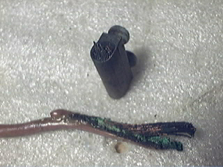
This was caused by a loose connection in one of the test loads...
That multi-stranded wire just fused 😱 it's no joke, the wire actually broke due to overheating.
This was caused by a loose connection in one of the test loads...
That multi-stranded wire just fused 😱 it's no joke, the wire actually broke due to overheating.
Really impressive...... do you want to go in the iperspace or you want to create an hole in the temporal space continuos... please advert us before you turn on your time machine 😱
Are you really using bipolar transistors as switches in the PSU? Or have I missed something?
Why aren't you using MOSFETs - especially for the rectification?
Why aren't you using MOSFETs - especially for the rectification?
I am using bipolar transistors for the full bridge switching stage and MOSFETs for the synchronous rectification stage.
I decided to use bipolars because there is no TO-220 MOSFET in the market rated at 400V Vds and capable of switching in excess of 10A with only approx. 1V voltage drop. On the other hand, modern switching bipolar transistors like MJE13009 yield that performance while providing reasonable switching losses.
Also note that each TO-247 MOSFET featuring 0.1 ohm Rds-on costs almost the same as a dozen of bipolar transistors and tnat kind of devices are very hard to drive because such a low Rds-on requires a huge die size with hugue capacitances, particularly the harmful reverse transfer capacitance.
The base drive circuit has gone a bit complex, but I'm happy because I get in excess of 1800W output with less than 40W loses in the bipolar full bridge. I'm trying to reach the 2KW mark in a reliable way.
Anyway, the circuit works fine at high powers, the problems I'm facing now are related to the complexity of average current control when only the primary side current waveform is available and it has a big switching peak at the beggining of each cycle (causing troble at very low duty cycles).
I use a pair of current transformers, one placed in each side of the full bridge, to get an isolated sample of the exact current waveform flowing in the primary side. I use two transformers because that allows to sense asymmetric currents. The main transformer is wound with a 12:1 turn ratio so 10A in the primary side must produce 120A output.
I also tried current transformers in the secondary side but I didn't like how it worked because transformer saturation was not sensed and compensated at all by the current loop. Also, it was harder to implement due to the hugue turn ratio required and the gauge of the secondary side magnet wires.
I also considered a hall effect sensor placed in the gap of the output inductor, but the cheap ones are too slow and the fast ones are so expensive that they may cost as much as the sum of the rest of the components of the PSU. Furhtermore, hall effect sensors in that arrangement would lose their measurement capability as the output inductor becomes saturated, so I discarded them idea.
- Status
- Not open for further replies.
- Home
- Amplifiers
- Power Supplies
- 0-15V 0-120A adjustable PSU attempt with average current control.