Hello!
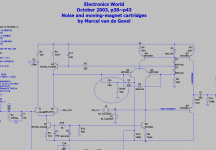
I've read Marcel van de Gevel's EW-2003 article "Noise and moving-magnet cartridges", I'd like to ask several technical questions about the schematic there.
I've read Marcel van de Gevel's EW-2003 article "Noise and moving-magnet cartridges", I'd like to ask several technical questions about the schematic there.
There are two errors in the article:
1. One of the sections of the switch in figure 5 is in the wrong state (Electronics World's mistake).
2. The terms spectral density and power spectral density are mixed up (my mistake).
Besides, the 3852 Hz rule becomes the 5179 Hz rule when you use ITU-R 468-weighting instead of A-weighting. ITU-R 468 is actually a better noise weighting curve than A-weighting.

The original article is
"Noise and moving-magnet cartridges", Electronics World October 2003, pages 38...43, https://worldradiohistory.com/UK/Wireless-World/00s/Electronics-World-2003-10-S-OCR.pdf
The extension to other noise weightings is derived in
https://linearaudio.net/grammophone-preamplifier-noise-calculations-3852-hz-rule-revisited
1. One of the sections of the switch in figure 5 is in the wrong state (Electronics World's mistake).
2. The terms spectral density and power spectral density are mixed up (my mistake).
Besides, the 3852 Hz rule becomes the 5179 Hz rule when you use ITU-R 468-weighting instead of A-weighting. ITU-R 468 is actually a better noise weighting curve than A-weighting.
The original article is
"Noise and moving-magnet cartridges", Electronics World October 2003, pages 38...43, https://worldradiohistory.com/UK/Wireless-World/00s/Electronics-World-2003-10-S-OCR.pdf
The extension to other noise weightings is derived in
https://linearaudio.net/grammophone-preamplifier-noise-calculations-3852-hz-rule-revisited
Last edited:
Goededag, lieve Marcel!
Thank you for your reply!
Yes, I noticed the switch error while doing my LTspice analysis.
My main question(s) is(are):
Thank you for your reply!
Yes, I noticed the switch error while doing my LTspice analysis.
My main question(s) is(are):
- why did not you use the drain current of J310 to control the current mirror that is almost already there - loading Tr1?
- and why the 3k01 (1%) is connected to the ground rather than to the negative power rail?
Connecting the 3.01 kohm to the negative power rail instead of ground would improve the voltage headroom for the second differential pair, but it would also produce a direct path from negative power rail ripple and noise to the input. Depending on the amount of ripple and noise and on the cartridge impedance, that may or may not be a problem. I used rather simple discrete voltage regulators with this circuit.
I don't see how connecting the 3.01 kohm to the negative rail could increase loop gain much, although it may increase it a bit through Early effect.
It's a circuit I designed some 30 years ago, so I may not remember every detail well, but regarding the JFET:
The J310 has a much lower voltage gain than a bipolar transistor, which means that calculating back to the input, ripple on its drain should lead to a worse equivalent input ripple than ripple on the collector of Tr1. Hence the filter in the drain lead of the J310.
The filter is also meant to drop the drain voltage by a few volt, because of the increase of JFET gate current and its noise when the JFET conducts current at high drain-source voltages (which is due to impact ionization, or so I've been told).
If your positive supply rail is clean enough and if you can get the drain voltage low enough, you could indeed improve loop gain with a current mirror. It will complicate the high-frequency behaviour somewhat, so you may need stronger frequency compensation. The current mirror will need emitter degeneration resistors for reasons of noise. This will worsen its high-frequency behaviour, but you could bypass the resistors with small capacitors to solve that.
I remember I considered using a common-mode loop in the second stage, similar to what I did in the line stage https://www.diyaudio.com/community/threads/tone-and-loudness-controls.405853/post-7567174 , to make the signal currents through the output BC558Cs closer to being equal but opposite. You now have an error due to base currents when their hfes are not exactly equal. In the end I didn't try that because of the PSRR issue and because the error is too small to worry about anyway.
Goededag, Marcel!
Thank you for the explanations.
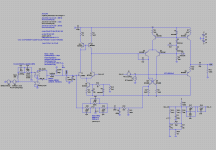
In the original schematic LTspice shows Id == 3,7mA (J310) and Ic == 2,5mA (Tr1).
To keep that ratio with the current mirror above the input diff, I had to arrange another mirror beneath the second diff. The loop gain increases approximately by 20dB, but the correction must be redesigned (I'm looking into that).

I don't understand why you would need a second current mirror when the first has a funny ratio.
Due to that second mirror, the output stage doesn't meet the port conditions anymore: the signal current flowing into the 3.01 kohm is no longer equal but opposite to the signal current flowing into the RIAA correction network. As a consequence, you will have to redimension the feedback network that sets the input impedance. The relation between the two currents may also be slightly non-linear, as it depends on the transconductances of Q10 and Q8.
Due to that second mirror, the output stage doesn't meet the port conditions anymore: the signal current flowing into the 3.01 kohm is no longer equal but opposite to the signal current flowing into the RIAA correction network. As a consequence, you will have to redimension the feedback network that sets the input impedance. The relation between the two currents may also be slightly non-linear, as it depends on the transconductances of Q10 and Q8.
Last edited:
I try to maximise the loop gain by all means possible.
The input impedance trimming is not difficult to be done later.
By the way, - what is your opinion about 75µs time constant being realised with the cartridge's inductance and preamp's input resistance?
In my particular case (Ortofon OMP40 with 450mH and 750Ohm) I need Rin == 5k25. I expect some noise penalty from that but in return I will have greater freedom with the cable's capacitance for the same frequency response allowance. Having preamp at tonearm's base is The Good Thing, but difficult to implement at certain TTs.
What's the point of increasing loop gain when you make the input impedance inaccurate and non-linear in the process?
When you look at figure 3 in my article, you see that you can in theory make the input impedance as low as you like without decreasing the value of the feedback resistor (so without increasing its thermal noise current) by increasing the gain K, but in practice, you can't make K too large because of headroom requirements. I therefore think you will indeed get a small noise penalty when you go for 5.25 kohm input resistance.
When you look at figure 3 in my article, you see that you can in theory make the input impedance as low as you like without decreasing the value of the feedback resistor (so without increasing its thermal noise current) by increasing the gain K, but in practice, you can't make K too large because of headroom requirements. I therefore think you will indeed get a small noise penalty when you go for 5.25 kohm input resistance.
That OPA1656 RIAA circuit is within .25 dB using a reverse RIAA circuit.
Download the data sheet , I used NJR2068 at 40 cents works very well.
Download the data sheet , I used NJR2068 at 40 cents works very well.
Yes, I understand that.you can in theory make the input impedance as low as you like without decreasing the value of the feedback resistor (so without increasing its thermal noise current) by increasing the gain K, but in practice, you can't make K too large because of headroom requirements.
I study your article and schematic because it is the most elaborate material I ever met on topic of noise in phono-preamps. Your circuit looks simple but it is surprisingly efficient.
My current preamp also has electronic cooling, the signal is taken at the output (the flat frequency response) so a RIAA-preemphasis network is required to drive the "frosen" resistor.
I want to learn from your approach and implement it in a circuit with LR75µs input, hopefully - without huge loss noise-wise.
Goededag, Marcel!
If I'm reading the article correctly, Tr1 should have Ic == 52µA. For some reason I do not see that in LTspice.
Is that because of a sub-par 2SC2545 model I have?
If I'm reading the article correctly, Tr1 should have Ic == 52µA. For some reason I do not see that in LTspice.
Is that because of a sub-par 2SC2545 model I have?
Code:
.model 2SC2545 NPN (IS=159.9F BF=578 VAF=121 IKF=1.43 ISE=10.52F NE=1.28 BR=27.4
+ VAR=50 IKR=10 ISC=1.622P NC=1.27 RE=1 RB=10 RBM=1 IRB=100U RC=10 CJE=60.37P
+ VJE=426M MJE=319M CJC=11.54P VJC=300M MJC=334M XCJC=500M VJS=700M MJS=500M
+ TF=279.5P XTF=1 VTF=1.105 ITF=999M TR=23N XTB=1.235 VCEO=60 ICrating=100m
+ MFG=Hitachi)

.model 2SC2546 NPN (IS=2.30174F BF=845 NF=784.9M VAF=190 IKF=434.2M ISE=35.2F
+ NE=1.3116 BR=10 NR=783M VAR=50 RE=1M RB=39.34 RBM=12.26 IRB=3M RC=700M CJE=79P
+ VJE=500M MJE=248M CJC=10.56P VJC=600M MJC=448M TF=328P XTF=17 ITF=600M TR=36N
+ XTB=1.54 VCEO=90 ICrating=100m MFG=Hitachi)

.model 2SC2547 NPN (IS=2.30174F BF=845 NF=784.9M VAF=190 IKF=434.2M ISE=35.2F
+ NE=1.3116 BR=10 NR=783M VAR=50 RE=1M RB=39.34 RBM=12.26 IRB=3M RC=700M CJE=79P
+ VJE=500M MJE=248M CJC=10.56P VJC=600M MJC=448M TF=328P XTF=17 ITF=600M TR=36N
+ XTB=1.54 VCEO=120 ICrating=100m MFG=Hitachi)Goededag, Marcel!
I un-did my current mirrors tweaks and tried to improve the loop gain in the original circuit solely by means of correction networks.
By replacing the single capacitor (15pF Ccb) with the T-network (5p6+3k6+15p) and changing 180+22pF in the feedback network to 470+100pF it was possible to prolong the 50dB shelf well over 20kHz.
Loop gain original:
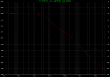
Loop gain tweaked:

Now I'm trying to refine the stability margins.
I un-did my current mirrors tweaks and tried to improve the loop gain in the original circuit solely by means of correction networks.
By replacing the single capacitor (15pF Ccb) with the T-network (5p6+3k6+15p) and changing 180+22pF in the feedback network to 470+100pF it was possible to prolong the 50dB shelf well over 20kHz.

Loop gain original:

Loop gain tweaked:

Now I'm trying to refine the stability margins.
75usLRinput is a bad idea -implement it in a circuit with LR75µs input
The question was about an electrically "cold" 5.25 kohm termination resistance, per post #10. KT315A and I both think there will be a noise penalty anyway, but much smaller than with a plain old 5.25 kohm resistor shunting the input.
yes, cooling helps minimize noise penalty of even as low Rin as 5.25k, but cannot helps with THD increase due to an almost -20 dB decrease in loop gain at frequencies above 2 kHz (75 μs) and frequency response error due to failure to take into account the strong frequency dependence of the loss resistance (as R* in table2 of your article @ EW 10\2003 - up to 30k @ 20kHz, how will it be chord with forming trivial but frequency dependent resistive divider with Rin 5.25k ?) and inductance L(f) of the MM cartridge.315A and I both think there will be a noise penalty anyway
Last edited:
Transfer from EMF to loaded voltage for a Shure V15-III with standard load (47 kohm // 450 pF), 150 kohm load and 4794.5333... ohm load, the latter with an extra zero at -13.3333... krad/s, all in dB normalized to 1 kHz, horizontal scale in Hz.

R*(f) in the table2 (by Richard Visee?) @ your "cooling article" still remain a stunning revelation. Maybe Richard has other interesting research?Transfer from EMF to loaded voltage for a Shure V15-III
which makes even more extra noise penaltythe latter with an extra zero at -13.3333... krad/s

Last edited:
If the 12 dB drop-off that you get with the recommended load is meant to compensate for some mechanical resonance, then the Shure V15-III is not suitable for 150 kohm load, nor for a RIAA amplifier that realizes the 75 us time constant by means of a 4794.5333... ohm load. Not without extra correction filters, that is.
- Home
- Source & Line
- Analogue Source
- I'm interested in RIAA preamps design