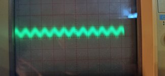
Greetings! I am building a GFA-565 amplifier, and the signal shown in the image is present at the amplifier's output. How much of an issue could this be for sound quality? Is it worth addressing this problem? Note that the amplifier is not yet installed in its case. The oscilloscope is set to 0.2 µs/div, 50 mV/div, and x1 probe position. The signal at the amplifier's output is approximately 20 MHz with an amplitude of 50 mV.
Attachments

Last edited:
Definitely should not be doing that. If you are building a clone, this could be caused by layout or device substitutions.
Is there a Zobel?
Is there a Zobel?
The amplifier is based on the GFA-565, 585, and Hoppe's Brain EBFA-565 designs. Some components had to be replaced. The output Darlington transistors are C4793, A1837, and NJW0302G, NJW0281G. The Zobel network is the original 47nF and 6.8Ohm.
Without a schematic, try reducing the bandwidth of the VA stage.
Also make sure the 6.8 Zobel resistor is non-inductive.
Also make sure the 6.8 Zobel resistor is non-inductive.
That is definitely ultrasonic oscillation. You must remove it. 3 pay sites offer the service manual, plus hifiengine which I chose not to sign up for. Elektrotanya download failed. So if you want help, post one channel schematic here.
To expand on post #4, put 47 or 51 pf capacitor C to B on voltage amplifier transistor. The second stage.
You might also put an inductor in the feedback line from the output to the base of the inner transistor of the input
"long tailed" pair. I use 5 or 6 turn ones salvaged from dead PC power supplies or LED TV's. Put the inductor near the transistor. You could instead wrap 5 turns insulated wire around a AAA battery, then remove the battery before installation. If the amp is for a band that sets up every night, put a drop of glue on the inductor you made to keep it stable.
Last edited:
Just for interest do see this oscillation if you short the probe tip and probe ground together and then touch the still shorted tip and ground lead to the amplifier ground you are using in the above picture?

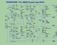
Here are the schematics and information: GFA-565/585 SCH and more.
Mooly: If I short the probe tip to the ground, no unwanted signal appears.
The driver board components are based on the EBFA-565. The output driver stage operates in Class A, similar to the GFA-585.

Mooly: If I short the probe tip to the ground, no unwanted signal appears.
The driver board components are based on the EBFA-565. The output driver stage operates in Class A, similar to the GFA-585.
I tried altering the Zobel network: using a 6.8Ω wire-wound resistor or a 7.5Ω metal oxide resistor. The issue persisted. Without the Zobel, the oscillation is reduced by a few millivolts.
Wirewound resistor probably inductive unless datasheet claims it is non-inductive. Metal oxide should not be inductive. 7.5ohm versus 6.8 ohm should not be a dangerous change on the zobel.
The feedback line is very long. Look at pin 7 of the input board. Goes to bases of Q105 and Q106. Could be coupling capacitively to the output. There I would put a little inductor to block RF to q105+106. Maybe lift one leg of R126 and put the inductor series that. I cannot read C105, maybe 82 pf? That should be small enough to not pass much 20 mhz, but I cannot read R126 either.
If that does not work, Q109 and Q110 are the VAS I believe. Could slow down slew rate there with capacitance C to b on both.
Why 10 pairs of output transistors? Was this designed prior to MJ15024/25? The rails have to be under +-100 v, the filter caps are rated for that. 35000 uf is enormous. I have a 650 w/ch amp with only 5 pairs of MJ15024/25. Rails were +-85 from 10000 uf caps. This appears to be obsolete. User manual says .1% clipping wattage is only 700.
Last edited:
This sketch provides better visibility.
This is an old amplifier with power ratings of 300W, 450W, and 850W for 8Ω, 4Ω, and 2Ω loads, respectively. Due to the low impedance handling, it employs many transistors. Its supply voltage is ±85V, but in my setup, it's ±75V.

This is an old amplifier with power ratings of 300W, 450W, and 850W for 8Ω, 4Ω, and 2Ω loads, respectively. Due to the low impedance handling, it employs many transistors. Its supply voltage is ±85V, but in my setup, it's ±75V.
Last edited:
I soldered a 47pF capacitor across the CE terminals of Q109 and Q110, but the oscillation did not change at all.
The second schematic shows 2 feedback resistors, R120 and R124. You may have to put in 2 inductors, on the bottom side of each. There is also a feedback path to IC101 the DC servo. If inductors on base side of R120+124 do not kill the oscillation you may have to do something about the op amp. If 5 turns don't help, try 10 turn inductors.
The chances of an individual matching 20 output transistors are pretty low. A factory can do it, their buys are big enough that the semiconductor company will do it for them. All transistors will come from the same production run. But an individual buying from a distributor gets Vbe and gain all over the map from different factory runs. Net result, 1 or 2 output transistors do all the work and overheat. The emitter resistors do not help the situation. .22 ohms is pretty minimal. Peavey used .5 ohm emitter resistors in the PV1.3k for better current sharing and they sell matched sets of replacement transistors for repair shops.
Update, slew rate limiting capacitors go C to B of VAS transistors.
Last edited:
I applied a 3.3uH THT inductor next to R120 and removed the servo IC, but the oscillation remains unchanged.
Recalculation. 82 pf is only 200 ohms to 20 mhz. So c105 and c106 allow more feedback at 20 mhz than the resistors. This is getting complicated. c105 c106 are compensation caps, and I cannot calculate compensation poles.
Maybe you could lift bases of Q105 106 and put the coil in there blocking all 4 feedback parts.
Maybe you could lift bases of Q105 106 and put the coil in there blocking all 4 feedback parts.
This looks like parasitic oscillation - not loop related. Loop related oscillation is almost always at or below 1 MHz. If you probe around the VAS and pre-drivers your scope does it change the frequency or the level? For this, leave the other probe connected to the output.
If two probes are connected, there is cross-talk between the channels on the oscilloscope. When I touch something with the other probe, the signal increases or decreases (whether it is a component in any stage or the output, for example). The frequency remains unchanged.
The amplifier is not shielded, and it is not in a case.
Update:
This is how the driver board signal looks without the output panel, with 2 x 1kOhm resistors in feedback. The oscilloscope is set to 1mV, 1µs, x1.
The amplifier is not shielded, and it is not in a case.
Update:
This is how the driver board signal looks without the output panel, with 2 x 1kOhm resistors in feedback. The oscilloscope is set to 1mV, 1µs, x1.
Attachments
Last edited:
It was worth checking. So it seems it is unwanted instability somewhere. Not easy to diagnose at a distance 🙁Mooly: If I short the probe tip to the ground, no unwanted signal appears.
I was afraid of this. I hoped it wouldn’t be a major issue since this is a production model. However, it is old, and many components in the circuit had to be changed. The new components were based on Phloodpants’ recommendations. I don’t think it’s a serious problem because the amplifier is working. Unfortunately, it’s difficult to pinpoint the exact source of the issue.
Post 7 has standard input pairs , post 10 has darlington pairs ?
Which is it ?
As far as a standard (Leach type) input stage driving that Hawksford (VAS) , this one of the most stable topologies.
NO oscillation even when I totally forgot C13/14 !!! With 22pF = 150+ V/uS ...
PS - "Phloodpants" ?? This guy upgrades Adcom's (Nice PCB's) , but he does not design them.
OS
Attachments
Last edited:
In the 7. post, there's a link that includes the service manual along with the parts list. The differential amplifier is always configured with a Darlington input (Mpsa13, 63), although this detail isn’t apparent in the schematic. Yes, Phloodpants from Hoppe's Brain—he has provided a wealth of useful information here on the forum and also on his website.
I can now see that the oscillation is also present on the collectors of Q110 and Q111.
I can now see that the oscillation is also present on the collectors of Q110 and Q111.
- Home
- Amplifiers
- Solid State
- Is this a case of noise or oscillation? How critical is the impact of this signal anomaly