Today I spent time improving the breadboarded version, playing with compensation changes the simulation suggested and its much less temperamental now:

Firstly square waves are cleaner at small and large signal levels:


And amplitude response is pretty flat to 100kHz, here's the 100kHz sine:

And 50kHz square:

In these the green plot is the input to the NIC stage, nominally a virtual ground. This signal is approximately a differentiated version of the signal as it has to drive the NIC VAS like a Miller cap - clipping shows up dramatically in this signal:


The behaviour of gross clipping seems devoid of oscillation or lock-up too, no doubt related to the cleaner handling of transient edges/square waves.
The agreement with simulation is closer too. I tried both NE5532 and LM4562 in the first position and no obvious difference in behaviour. I'd like to try NE5534A and find out what compensation is needed for it, but the different pinout means redoing the breadboard a bit.
So I'm thinking this topology in this form is work taking forward, standard parts and passives and no specialist audio transistors needed except the output section.
Firstly square waves are cleaner at small and large signal levels:
And amplitude response is pretty flat to 100kHz, here's the 100kHz sine:
And 50kHz square:
In these the green plot is the input to the NIC stage, nominally a virtual ground. This signal is approximately a differentiated version of the signal as it has to drive the NIC VAS like a Miller cap - clipping shows up dramatically in this signal:
The behaviour of gross clipping seems devoid of oscillation or lock-up too, no doubt related to the cleaner handling of transient edges/square waves.
The agreement with simulation is closer too. I tried both NE5532 and LM4562 in the first position and no obvious difference in behaviour. I'd like to try NE5534A and find out what compensation is needed for it, but the different pinout means redoing the breadboard a bit.
So I'm thinking this topology in this form is work taking forward, standard parts and passives and no specialist audio transistors needed except the output section.
After a while I have been getting round to assembling my prototype NIC topology amps with a with to boxing them with a power supply - an excuse for a few more pictures, showing the simple heatspreader bar arrangement which was a consequence of rooting about in my aluminium extrusion pile and finding no thick angle sections, so choosing 25mm square bar instead:

This sort of deep drilling mandates using a pillar-drill, and lubricant to prevent friction from grabbing the drill bit. Rather than tap the holes I simply drilled through, recessed on one side and used long M3 bolts.


Further testing to follow once its got its PSU is the plan. The heat spreader has enough thermal mass for short-term testing before I select a final heatsink and enclosure, which is handy.
This sort of deep drilling mandates using a pillar-drill, and lubricant to prevent friction from grabbing the drill bit. Rather than tap the holes I simply drilled through, recessed on one side and used long M3 bolts.
Further testing to follow once its got its PSU is the plan. The heat spreader has enough thermal mass for short-term testing before I select a final heatsink and enclosure, which is handy.
Spice models
I had a similar problem with the "level 1" (*.301) model of TLE2071 but the level 2 (*.302) model worked OK.
I think this is the closest sim to what I've built (I keep tinkering).
I use LT1028's in the sim because the 5532/5534A models I have are slow to emulate (or don't converge) in heavily fedback arrangements it seems.
I had a similar problem with the "level 1" (*.301) model of TLE2071 but the level 2 (*.302) model worked OK.
messing with your amp
I played with this and found that the reason your simulation file does not latch up is, that it clips at 38V /48V, probably because of the latfets. If you reduce the load to 100 Ohms, your circuit latches up. The ratio of the feedback on U2 would be safer if a 48V output was reduces to less than the op-amp rail, so the inputs remain between the rails. I replaced the FETs with VFets and it just latched up until I changed R9/R10 and R13/R14.
And infinity gain at U2 is probably a bad idea, so I changed R14/R13 so that the gain is finite. I fiddled with it some more and the attached is where I'm at at the moment.
Attachments
Thanks for your feedback (sic!). I'll have a another look at this soon when I get time. BTW U2 doesn't have infinite gain as I view it as the circuit is not being used as a voltage amp but more like a transimpedance amp (its gain is 30k ohms in my version).
So you can think of U1 having the high gain, as its a transconductance amp with open-loop gain of A / Zout, where A is the open loop voltage gain, Zout the open loop output impedance (this ratio falls rapidly at high frequencies as open loop gain drops and impedance rises)
You can make R14 larger than R10 and still have it work - the voltage at the output of U1 is then reversed, but since its the current signal that matters that's not a big issue. This is an area where simulation doesn't seem to work well, simulation doesn't like R14 larger than R10 probably due to the open-loop output impedance of U1 not being represented well? Anyway this mode is interesting as the (current) feedback is working in the opposite direction to the voltage at that node - its quite counter-intuitive!
Its interesting to note that without the outer feedback loop the NIC stage would have to be like your version with "finite voltage gain", unless current-driven.
Mark, I think there is something to the 'infinite gain' viewpoint. That NIC opamp has the same positive feedback as negative feedback. As a stage, ideally, this means it has infinite gain internally, but gain as set by the resistor values, to the outside, and would be sensitive to small value deviations causing instability. The 5pF in your circuit helps stability.
You can view the whole amp as having an infinite gain stage inside the feedback loop leading to a very high feedback factor and that would explain the extremely low distortion as reported above.
A very interesting and intriguing concept!
Jan
You can view the whole amp as having an infinite gain stage inside the feedback loop leading to a very high feedback factor and that would explain the extremely low distortion as reported above.
A very interesting and intriguing concept!
Jan
Last edited:
I've been looking at Nyquist plots in simulations of this and convinced myself that R14>R10 or R14<R10 makes no great difference to the stability, even though in one case the open loop DC gain is negative and in the other positive - or even if its infinite.
I note the distortion seems lowest with R14>R10, where the output of U1 is inverted, although this worsens the recovery time from clipping.
I note the distortion seems lowest with R14>R10, where the output of U1 is inverted, although this worsens the recovery time from clipping.
So I figured out a way to get Nyquist plots with logarithmic scaling (by exporting from LTSpice and processing in Python), so here are the plots for the two cases:


The black circle is the unit circle, and the red dot the point (-1, 0) for the Nyquist criterion. Outside the unit circle the magnitude of the response in the plot is scaled to ln(x)+1, and inside to -1/(ln(x)-1) - the angle/phase is unaffected.
The lack of clockwise encirclement in each case indicates stability...
And its clear the response at higher frequencies tends to the same behaviour in and around the unit circle (presumably the capacitors in the NIC network ensure this). And thus the low frequency response is not affecting stability (even the reversal of DC gain's sign, or presumably it going to infinity).
In otherwords the low frequency gain of the open loop is not actually interesting to closed-loop behaviour/stability, so long as its magnitude is large.
Last edited:
Yes, looks stable Mark, good. Is it too much to ask for a zoom in on the Nyquist diagrams, like from -2 to +2? Sometimes there's some detail that is lost in the large view.
Jan
Jan

Yes, thanks, it shows the wild gyrations of the phase at high frequencies.
But that has no consequences of course, engineering curiosity only ;-)
Jan
But that has no consequences of course, engineering curiosity only ;-)
Jan
I'm hoping to have some time to do some proper measurements (with my new QA403) on my NIC amp over the holidays, but first I'm reposting the diagram lost from #33:

So I've got round to testing the physical embodiment of this NIC based amp of mine (unloaded), Approx +/-45V supplies, having now got a QA403 audio analyzer.
First distortion v. input level plot at 1kHz:

Which seems respectable - whether it can maintain this under load has to wait for me to dig out the bigger PSU and dummy load to test.
And distortion v. frequency at -5dBV input level:

The glitch at the end is the third harmonic going out of range - this mode of measurement seems not to allow setting a measurement BW.
Clearly distortion would be rising from 6kHz or so. I'm running the QA403 at 192kSPS BTW. The low frequency rise may be inadequately sized bootstrap caps?
FYI the amp gain is 30dB, so -5dBV in means 25dBV out (18Vrms). The amp clips unloaded at about -1 to 0 dBV input.
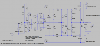
And here's the as-build circuit (or close to it) I believe:

The opamps are actually NE5534A's (I couldn't get the simulation to run with those models alas), and the outputs are Exicon's, not Hitachi. I believe the input network is a bit more complex on the PCB, and the first opamp supply is zener based, I can dig out the actual PCB schematics too if interested.
First distortion v. input level plot at 1kHz:
Which seems respectable - whether it can maintain this under load has to wait for me to dig out the bigger PSU and dummy load to test.
And distortion v. frequency at -5dBV input level:
The glitch at the end is the third harmonic going out of range - this mode of measurement seems not to allow setting a measurement BW.
Clearly distortion would be rising from 6kHz or so. I'm running the QA403 at 192kSPS BTW. The low frequency rise may be inadequately sized bootstrap caps?
FYI the amp gain is 30dB, so -5dBV in means 25dBV out (18Vrms). The amp clips unloaded at about -1 to 0 dBV input.
And here's the as-build circuit (or close to it) I believe:
The opamps are actually NE5534A's (I couldn't get the simulation to run with those models alas), and the outputs are Exicon's, not Hitachi. I believe the input network is a bit more complex on the PCB, and the first opamp supply is zener based, I can dig out the actual PCB schematics too if interested.
Last edited:

I've tested the amp again with 8 ohm dummy load, and alas distortion pops up - presumably from the output stage asymmetry (investigations show its predominately even harmonics):

(The orange plot is unloaded)
Clearly the global loop is running out of gain to correct the OS distortion quite early - its about 12dB per octave.
(The orange plot is unloaded)
Clearly the global loop is running out of gain to correct the OS distortion quite early - its about 12dB per octave.
I measured the output stage on its own, about -80dB unloaded, -40dB with 8 ohm load, so I think that 12dB/octave is the combined roll off of the two opamps in the NIC amplifier. I think this design requires a more linear OS to shine.
The circuit in post #36 has about 48V on U2 output and supply pins with 1/3 that, about 16V on the inputs, ie +/-32V common mode; too much. Swapping R9 and R10; R13 and R14 is almost enough to fix the problem.
Not in my simulations nor in the real circuit - U2 is bootstrapped to follow the output with a little attenuation, keeping its input and output pins within its supply range. It the outputs are 45V or so the inputs are 15V or so - remember this is really an NE5534A with +/- 18V supplies
- Home
- Amplifiers
- Solid State
- NIC opamp VAS topology