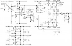
Intended to learn simulation, this amplifier schematic comes up. Yes, it's a modification from some schematic around internet. I did use Micro Cap 12 to simulate. The simulation result looks like output power = 21.1W (RMS) and THD is about 0.02% when D1/D2 being 1N4749. The quiescent current for each output transistor is about 975mA, if my simulation is not so wrong.
There is a significant question to be asked here: is this safe to use +/- 19VDC or even +/- 21VDC for NE5532A for listening? because according to NE5532A specification from TI, its absolute power supply is +/- 19VDC.
Is this Class-A BJT amplifier schematic worth a tryout? Do you think there is a better schematic to try? Under consideration of utilizing NE5532A for voltage gain and DC servo, and SC5200/SA1943 as output transistors. BTW, for learning purpose I already used KiCAD 6 to get a PCB layout and routed, about 2.5"x7", not send out for PCB sample manufacturing yet. I know there are so many DIY experienced people around here, that's the reason I am asking. Don't laugh at me.
Attachments
Nope, it looks like an "under biased" class B.
The bias voltage is set by the ratio of R8 and R22 and it is less than the 4 Vbe necessary to turn on the output stage.
The bias voltage is set by the ratio of R8 and R22 and it is less than the 4 Vbe necessary to turn on the output stage.
Notice that you can't drive the output devices' Bases all the way to the power rail, if you run the '5532 on a reduced voltage.
https://www.ti.com/lit/ds/symlink/ne5532a.pdf

Hmmm, not what I see. I don't recall 19V on any opamp.according to NE5532A specification from TI, its absolute power supply is +/- 19VDC.
https://www.ti.com/lit/ds/symlink/ne5532a.pdf
I can't decide that for you. If you are looking for a not too complicated class A design you can look at Nelson Pass. If you want to design something yourself, reading a book is best start imo, for example the appropriate books of Bob Cordell and Douglas Self
Hi. You can test this scheme in practice if you want.Do you have a better schematic which have VAS?
https://www.diyaudio.com/community/...man-has-no-memory.318989/page-44#post-7229429

Yes, I am learning including to read the books, which including the Bob Cordell and Douglas Self book. From engineering perspective, why not use the good sound NE5532 or NE5534, also I like Toshiba TTC5200/TTA1943. This push me starting to think how to put those components together.I can't decide that for you. If you are looking for a not too complicated class A design you can look at Nelson Pass. If you want to design something yourself, reading a book is best start imo, for example the appropriate books of Bob Cordell and Douglas Self
Last edited by a moderator:
I want to try your schematic at some point. Thank you for the help.Hi. You can test this scheme in practice if you want.
https://www.diyaudio.com/community/...man-has-no-memory.318989/page-44#post-7229429
Similar amp that works for sure:
https://www.diyaudio.com/community/threads/latfet-amp-based-on-philips-ah578.367494/
https://www.diyaudio.com/community/threads/latfet-amp-based-on-philips-ah578.367494/
R8 and R22 look interchanged. With that fixed, this seems like a working amplifier but not great due to the inability to swing close to the rails.
Ed
Ed
If it is, then Q5 is burned out. Vbe of a good silicon transistor will be in the 0.60 - 0.65 volt range.@anibal
Thank you for the reply. Vbe(Q5) is about 5.2VDC, that's larger than 4Vbe(~3V). Wrong calculation?
Hi Wilson@anibal
Thank you for the reply. Vbe(Q5) is about 5.2VDC, that's larger than 4Vbe(~3V). Wrong calculation?
First of all, I have used pretty similar circuits many times and they work OK, you may think it as an opamp with a power buffer output stage.
Definitely there is an issue and then few details that may improve it.
Regarding the bias, the voltage across Q5 is Vbias=Vbe (R8+R22)/R22; probably the mistake is swapped positions of the resistors.
I do not know your target, I guess the no global feedback is intentional, but if you change R3 taking signal from the output you will get much lower THD.
If you want to introduce a meaningful change in "perceived audio quality" I suggest the following mod:
Remove R27 and replace R10 with a constant current source of about 5 to 10mA, the 5532 has a quasi-complementary output stage (only NPN transistors) so making this mod you will force the opamp to work in class A with only its "upper" output transistor active.
Anibal
P.S.:
If you go for the current source, please connect it to Ve instead of Vee.
R28=4.7ohms has no meaning in the input circuit wired as it is, if you want to keep it to avoid ground loops you should change the connection of R4=680 from GND to the common point of R2, R28 and C1.
Finally, your bias generator is "OK", but it pretty basic and can be improved.
Good luck🙂
@anibalHi Wilson
First of all, I have used pretty similar circuits many times and they work OK, you may think it as an opamp with a power buffer output stage.
Definitely there is an issue and then few details that may improve it.
Regarding the bias, the voltage across Q5 is Vbias=Vbe (R8+R22)/R22; probably the mistake is swapped positions of the resistors.
I do not know your target, I guess the no global feedback is intentional, but if you change R3 taking signal from the output you will get much lower THD.
If you want to introduce a meaningful change in "perceived audio quality" I suggest the following mod:
Remove R27 and replace R10 with a constant current source of about 5 to 10mA, the 5532 has a quasi-complementary output stage (only NPN transistors) so making this mod you will force the opamp to work in class A with only its "upper" output transistor active.
Anibal
Thank you very much for the time writing the detailed suggestions. You kindness and effort are greatly appreciated.
Modification will be taken as 1) remove R28 (4.7Ohm); 2) remove R27 (3.3K) and replace R10 with 10 mA constant current source with connecting to Ve. 3) R8 (500ohm) and R22 (2.2K) will be swapped.
@YlliIf it is, then Q5 is burned out. Vbe of a good silicon transistor will be in the 0.60 - 0.65 volt range.
you are right, Vbe is 0.7V. But the Q5 is not burning yet because it's on the schematic only.
@EdGrR8 and R22 look interchanged. With that fixed, this seems like a working amplifier but not great due to the inability to swing close to the rails.
Ed
Yes, they will be swapped. 🙂
The voltage swing at the output of the NE5532 is to low to drive the emitter-follower output stage. Considering the given Vcc / Vee of +32 / -32V, it's burning energy at no purpose. Even more when run in class A. That's why I wrote you are missing a voltage amplifier stage.Yes, I am learning including to read the books, which including the Bob Cordell and Douglas Self book. From engineering perspective, why not use the good sound NE5532 or NE5534, also I like Toshiba TTC5200/TTA1943. This push me starting to think how to put those components together.
- Home
- Amplifiers
- Solid State
- Is This Class-A BJT Amplifier Schematic Worth A Tryout?