I built a simple single ended tube amp kit based on EL34. The PSU contains a capacitance multiplier circuit. After a few hours playing, the IGBT chip blew (shorted). I need to figure out what causes the failure before buying a replacement part. Can someone help to identify the issue or suggest changes to the circuit?
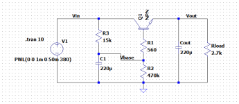
The circuit of the PSU is below. The actual supplied part for Q1 is FGA25N120, which is a 1200V, 25A NPT Trench IGBT with build-in protective diode. It was mounted on a heat sink. The size of the heat sink is 22 X 35 X 15 mm.


When the unit was working, voltages at C, G, E were 314.5, 305.2, 292.7V. The amp consumes about 140 mA. So the IGBT is dissipating around 3 watts.
My questions are:
The circuit of the PSU is below. The actual supplied part for Q1 is FGA25N120, which is a 1200V, 25A NPT Trench IGBT with build-in protective diode. It was mounted on a heat sink. The size of the heat sink is 22 X 35 X 15 mm.
When the unit was working, voltages at C, G, E were 314.5, 305.2, 292.7V. The amp consumes about 140 mA. So the IGBT is dissipating around 3 watts.
My questions are:
- Why choose IGBT while other designs use MOSFET or Darlington? Is IGBT less reliable or I just got a bad part? Should I switch to a MOSFET?
- Does the design dissipate too much heat or cannot handle start up? I tried to turn on heaters for 15 seconds before turn on the power, but not always so.
- Is the heat sink too small? If so, how big should it be?
- Every capacitance multiplier is a bit different. However, is this one a good design? I found the use of three 220 uF capacitors in this circuit is a bit excessive. In fact, I now took the IGBT out and connect the capacitors in a simple CRCRC filter. R1 is 82 ohm and R2 is 37.5 ohm. I got B+ at 301V with only 0.5 mV hum at the speaker output. Looks like the capacitor multiplier is not even needed.
Drawing says G40N150D, maybe your actual part is lower rated.
The part in the drawing is rated for 40A, so that(and small heat sink) may be the reason for failure.
The part in the drawing is rated for 40A, so that(and small heat sink) may be the reason for failure.
It is unlikely that Q1 died because of overvoltage or overcurrent, unless you shorted something while working on it.
You mentioned a protection diode on the base/gate. Those are meant for ESD protection but can be ineffective to limit the voltage encountered in an actual circuit.
For real protection you should use an actual external zener diode.
I've been bitten by that a few times before someone told me this.
Jan

I think the last cap of 220uF is too big
Try to put a 100 ohm 3w resistor in series with emitter to a cap
Try to put a 100 ohm 3w resistor in series with emitter to a cap
When using as a cap multiplier, which is a follower structure, IGBTs work almost the same as MOSFETs.
Generally IGBTs will have higher breakdown voltage and higher capacitance comparing with MOSFETs.
I think the reason why your IGBT broken is C1. I can't figure out anything about internal protection zener in the datasheet. When turn off the power, the voltage on C0 and C3 will drop quickly due to the tube's cathode is still hot enough.
Pay attention to C1. Since it's a RC filter. There's no way for C1 to discharge as fast as C0 and C3, and you're useing an extremely large capacitor here.
When the switch is turned off, the voltage on C3 will drop quickly, which increases the Vge and force the IGBT entering further ON-State, so C0 will drop at the same speed as C3.
But the C1 can't discharge fast. The total resistance for it to discharge is about 15Kohms, while it's about 2.2Kohms for the C0 and C3 to discharge (300V 140mA).
The voltage difference between C1 and C3 is applied directly on Gate and Emitter. With the fast discharge of C3 and slow discharge of C1, the Vge of the IGBT could easily go beyond 20 Volts and breakdown the insulation between Gate and Emitter.
Similar breakdown issues will occur when using MOSFETs.
So an external protection zener connected between Gate and Emitter (or Gate and Source of a MOSFET) is necessary.
The Gate-Emitter Voltage of the IGBT is ±20 Volts, and the Vge(th) is 7.5 Volts maximum, so I think you should connect a 12 Volts zener between Gate and Emitter for protection.
The zener will provide a path for the RC circuit to discharge fast, and limit the voltage between Gate and Emitter.
Such problem won't happen when using Darlinton transistors, since Base to Emitter is a series of 2 diodes. Although it's not common, adding a diode reverse to the two emitter junction will provide further protection against an Base to Emitter reverse breakdown.
You can search "Heat Sink" in Mouser, RSonline, Digikey, etc. Although heat sinks there are expensive, they will provide detailed datasheet which always contains the information you need calculating temperature of the power transistors. Just find similar products is enough.
For example this one.
https://www.mouser.cn/datasheet/2/670/hse_bx_035h_01-1777730.pdf
It's said that the thermal resistance is about 15°C/W.
3W on the power transistor means a temperature rise of 45°C on the heat sink.
Adding the thermal resistance of the power transistor (RθJC Junction to Case)
3W dissipation on a TO-247 package means about 2°C between case and junction.
Finally the thermal conductivity of your thermal pad between the heat sink and power transistor.
3W dissipation on a 1W/(m·K) 0.1mm thickness thermal pad means about 6°C between case and heat sink.
Add all of them, finally, you'll get a temperature rise of 53°C from junction to ambient.
If the maximum temperature inside your amplifier is 45°C, the junction temperature will reach about 98°C.
It's still safe, but a little bit high, which may affect long term reliability.
Last edited:
Thanks for the excellent feedback!
I did some further search and found this comment on BJT from Merlinb in the past "The secondary breakdown of BJTs is also a severe handicap as inrush current to subsequent filter capacitors can blow the transistor at start up." With a 220 uF capacitor right after the IGBT in the original design, this might be a concern.
I also found the attached E-Choke drawing. Looks like a 16 ohm resistor is inserted in the zener to reduce the inrush current.
You can use simulations to help you judge whether the transistor entered "secondary breakdown" area.Thanks for the excellent feedback!
I did some further search and found this comment on BJT from Merlinb in the past "The secondary breakdown of BJTs is also a severe handicap as inrush current to subsequent filter capacitors can blow the transistor at start up." With a 220 uF capacitor right after the IGBT in the original design, this might be a concern.
I also found the attached E-Choke drawing. Looks like a 16 ohm resistor is inserted in the zener to reduce the inrush current.
View attachment 1073970
There's 3 main limitations of Safe Operating Area. Voltage, Current, and Total Power Dissipation.
Just tracking the Vds, Ids and Pd using simulation softwares, compare the top of them to Safe Operating Area with certain duration limit.
It's not a common problem with IGBTs, since almost all of them have a high power dissipation ability.
In most situations, calculating the maximum allowed power dissipation of High Voltage DC operation in Safe Operating Area, and comparing it to your simulation. That's enough.
A large capacitor after the cap multiplier can be applied together with a slowly established voltage reference, and a large enough transistor with heat sink strong enough to withstand the heat dissipation during start up.
The E-Choke is another thing. And I havn't inspected further into it.
The resistor connected at the Source limits the current by providing Negative Feedback. It's more than just a series resistor.
That (post #8), and also I would let Tube filament to warm up at its own pace on startup; preheating it is actually the opposite of what´s needed/safer.
Besides that, not sure why an IGBT was used there, MosFets are perfectly good for that job and they do not have second breakdown problems as bipolars do.
Small rant follows: I understand IGBTs were designed to handle monster voltage and current needs, such as in subway electric motors, etc, but to me they are a kludge.
And if not FORCED to use them, avoid them.
Actually, MOSFETs do have 2nd-breakdown type issues.
NASA found out the hard (and expensive!) way. Google 'Spirito effect'.
https://www.nasa.gov/sites/default/...stability-1-28-10_NRB_TECH_BULLETIN_FINAL.pdf
Jan
NASA found out the hard (and expensive!) way. Google 'Spirito effect'.
https://www.nasa.gov/sites/default/...stability-1-28-10_NRB_TECH_BULLETIN_FINAL.pdf
Jan
From the datasheet of the IGBT you have used:
“Once the gate is triggered the IGBT will remain on even after the trigger voltage is removed similar to a MOSFET. This is because of the gate capacitance present on the input gate pin of IGBT. To turn off the device the gate capacitance has to be discharged by simply connecting the gate pin of IGBT to ground. Because of this normally the Gate pin of IGBT is connected to ground though a pull down resistor of 10k or a gate driver IC like IR2104 is used.”
I don’t see anywhere that this IGBT is suited for use in a linear operation (not switching). I know it can work nevertheless, but not always foolproof.
Certainly you will need an external zener (12V).
I’ve built a somewhat similar MOSFET circuit for 600 VDC with 1000 uF before the capacity multiplier and 2uF for C1 and 200 uF on the output.
I’ve had my issues too with “switchers” and changed to a MOSFET suited for linear operation.
Regards, Gerrit
Hi Gerrit, can you name one or more MOSFET suitable for linear operation?
I am actually thinking about ditching the original design and use the design Menno van der Veen published in May 2018 Glass Audio.
He chose SPP04N80C3. It is available at Digikey. There is also a isolated version but is in back order.
I guess 800V 4A is enough for the job.

I am actually thinking about ditching the original design and use the design Menno van der Veen published in May 2018 Glass Audio.
He chose SPP04N80C3. It is available at Digikey. There is also a isolated version but is in back order.
I guess 800V 4A is enough for the job.
Hi,
I've used the IXTH12N100L Linear Power MOSFET with "Extended FBSOA N-Channel Enhancement Mode Avalanche Rated".
I'm sure it's overkill in some (or many) ways, but so far it has survived all my experiments.
Regards, Gerrit
I've used the IXTH12N100L Linear Power MOSFET with "Extended FBSOA N-Channel Enhancement Mode Avalanche Rated".
I'm sure it's overkill in some (or many) ways, but so far it has survived all my experiments.
Regards, Gerrit
Don't use the isolated version, it has a much smaller SOA.Hi Gerrit, can you name one or more MOSFET suitable for linear operation?
I am actually thinking about ditching the original design and use the design Menno van der Veen published in May 2018 Glass Audio.
He chose SPP04N80C3. It is available at Digikey. There is also a isolated version but is in back order.
I guess 800V 4A is enough for the job.
View attachment 1073990
Jan
$22.07 for IXTH12N100L at Digi-key!
Some suggested FDP12N60NZ used by Jan. $2.18 at Digi-key.
Mouser has SPP04N80C3 at $2.17. Digi-key no longer has any in inventory. Lead time is 65 weeks.
I also saw someone mentioned using IRF820 and was quite happy with it. Is it still a good choice? The price for IRF820PBF is $1.47 and have plenty of them.
The FDP12N60NZ is end-of-life, get them while you can! I haven't been able to find an atternative with the same SOA area.
The IRF820 should also work well here. I don't know that other device, but 1000V is overkill and you pay for it with the other specs.
I use the FDP12N60 because it has to withstand 400mA @ 500V for half a second, that is one hell of an SOA requirement.
In the OP's application, the '820 will work fine, there's no large SOA requirement because the output voltage comes up relatively slowly so the inrush current into the output cap is low. I don't believe it blew due to inrush current, although I think the OP hasn't said which device he actually used. Or did I miss it?
LTspice can give a good approximation.
Jan
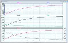
The giveaway is the long delay at the base. That limits the rise of Vout and thus the inrush current. It takes more that 10 secs for the load current to get up to 130mA or so.
You could use a simple TO-126 device here with no problems.
Jan
You could use a simple TO-126 device here with no problems.
Jan
Attachments
With an existing amplifier, with existing power transformer, etc., there often is not much to be done in the way of modifications.
But, when designing an amplifier from the ground up, and with new parts:
Here is just one way to look at power supply design. You might consider this to be a joke, depending on how perfect you want your power supply to be.
All my SE and Push Pull (and soon, a new design will be balanced) vacuum tube amplifiers have “regulated” supplies:
My power mains provider keeps the voltage between 117VAC and 123VAC.
120VAC - 2.5% = 117VAC
120VAC + 2.5% = 123VAC
(I design the power supplies for 120VAC)
+/- 2.5%, is not the best regulation, but not too bad for a starting point.
All the rectifiers are solid state: silicon diodes or HEXFREDs.
Pretty constant voltage drop versus load, not like a vacuum tube rectifier.
The B+ filters are either low DCR, greater than critical inductance choke input filters; or sometimes with a small input capacitor, 1uF to 4uF before the low inductance greater than critical inductance choke.
Typically, the choke output is followed by 100uF or 200uF, and then a 100 Ohm or 180 Ohm resistor to either a 200uF or 500uF cap to run the output stage. A 1k Ohm from there to a 100uF or 200uF cap runs the driver / phase inverter stage(s).
The large capacitance keeps the power supply voltage from varying on most music (the Telarc 1812 with a real canon 6Hz signal is one exception).
The capacitive reactance, Xc of a 500uF cap is 53 Ohms at 6Hz. Compare a 53 Ohm stiff B+, versus a 3k output transformer primary, or a 1k output tube plate resistance, rp.
Well, yes, the inductive reactance, Xl of the 3k output transformer is going to be far less than 3k Ohms.
How well do your loudspeakers work at 6Hz, and I bet the impedance = DCR at 6Hz (usually 1/2 of the ‘rated’ loudspeaker impedance).
My amplifiers are not high current ones, so the choke DCR series resistors between capacitors are of small effect with the change in load current versus signal level. The power transformer primary DCR and secondary DCR may be as much a factor as the rest of the series resistances.
Brute force B+, but since all output tubes input /driver / phase inverter tubes are self biased, the 2.5% B+ does not cause the stages quiescent currents to vary much.
As to designing an output stage for the perfect quiescent current and B+ voltage, consider that most loudspeakers are not like a non-inductive power resistor. So, in the real-world, there is no 'ideal' operating condition for the output stage across the 20Hz to 20kHz frequency range; the load varies over a wide range of resistance, capacitive reactance, inductive reactance, and combination of them.
Perfection should be aimed at, but can never achieved.
Just my opinions
Last edited:
- Home
- Amplifiers
- Tubes / Valves
- Blown IGBT in an EL34 Tube Amp Kit - what is the cause?