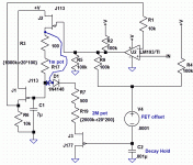
I am designing a VCA compressor (mostly for the bass guitar) based on a THAT4301 chip and am presently on the sidechain attack decay circuit. The design started with a circuit from a THAT comp pedal design, but quickly went elsewhere (I wanted adjustable time constants, which is turning out to be the tricky part).There design uses 2 BJT current sources feed a cap, one for attack the other for decay. The problem is that if the decay is adjusted to fast it changes the slower attack times. The decay ccs is draining enough current from the attack ccs to change the attack times. So I found a way to turn the ccs's on and off but still had its problems. Ended up using FETS to switch the currents instead. The hard part is getting the large ranges. Attacks can be between .01ms and 300ms and decays form .02s to 3s. getting these broad ranges (6 orders of magnitude) from 1 timing cap aint easy. The present circuit uses the FETs as dynamic resistances to help the pots change the currents.
Now the question. How much will these dynamic resistances (the FET properties) change with individual FETs (one J113 to the next ). Seems that different Vp of the same FET will change the timing current. Does this spec vary a lot ? How close to reality is this sim?
Thanks in advance.
Now the question. How much will these dynamic resistances (the FET properties) change with individual FETs (one J113 to the next ). Seems that different Vp of the same FET will change the timing current. Does this spec vary a lot ? How close to reality is this sim?
Thanks in advance.
Last edited:


I'm anything but a JFET expert, but... The pinch-off voltage can usually vary substantially between FETs of the same type. The datasheet normally specifies how substantially.
Well thats inconvenient. This isnt going into production so I think I can tweek the individual FETs with the dividers on the gates??? Does V4 replicate the Vp variance? Is this sim close to reality?
decay ccs is draining enough current from the attack ccs to change the attack times.
Normally, for speech/music compression, the decay pot/CS goes BEFORE the attack pot/CS.
Attachments
Last edited:
Let me try to reverse engineer your circuit first:Well thats inconvenient. This isnt going into production so I think I can tweek the individual FETs with the dividers on the gates??? Does V4 replicate the Vp variance? Is this sim close to reality?
If I understand the circuit correctly, then J2 is an N-channel source follower that is used for the attack together with R3 and R17. J3 is a P-channel source follower used for the decay together with R19, R7 and D1. C1 sets the time constant together with the various resistors. I'm not sure what C2 is for, and J1 is an N-channel source follower that buffers the voltage of C1.
The gate of J2 gets switched between roughly 0 V and 5.4 V by open-collector milspec comparator U2; do you play the bass guitar at temperatures below -40 degrees or is the macromodel named after the comparator version with the widest temperature range? The gate of J3 gets switched between roughly 4.5 V and 7.2 V.
I'm not sure about this because I don't understand C2, but I guess you want to prevent simultaneous conduction of J2 and J3. If so, then why don't you switch their gates all the way between 0 V and 9 V?
In any case, https://eu.mouser.com/datasheet/2/308/MMBFJ113_D-1811481.pdf specifies a VGS(off) between -0.5 V and -3 V for a J113 at room temperature. The SPICE model presumably models a typical value somewhere halfway in this range, so you have to count on +/- 1.25 V around the SPICE model value. For a J177, that's +0.8 V to +2.25 V according to https://www.nxp.com/docs/en/data-sheet/J174_175_176_177_CNV.pdf , so +/- 0.725 V around the SPICE model value. You can check the effect of pinch-off voltage spread by either tweaking the SPICE model parameters, or leaving the model parameters as is and putting a voltage source of +1.25 V, -1.25 V, +0.725 V or -0.725 V in series with the gate lead.
With the gate of J2 at 0 V, you need 3 V at C1 to get J2 at the edge of pinch off, if the VGS(off) happens to be -3 V. With 7.2 V at the gate of J3, it is only pinched off reliably up to 4.95 V of source voltage. With 9 V at the gate, that would be 6.75 V of source voltage. Thanks to D1, the voltage across C1 can go 0.5 V or so higher.
The range is likely to be narrower than I calculated because JFET pinch-off doesn't happen abruptly. How well or how poorly that is modelled is something you could check by simulating a single JFET, just put a few volts between drain and source, DC sweep the gate-source voltage and look at the drain current. If you see the current near pinch-off change by more than a factor of about 10 per 60 mV of gate-source voltage change at room temperature, the result is unphysical.
What range of voltages across C1 do you actually need? Is there any reason why J1 has to be a source follower and not an op-amp with JFET input?
Within a specified range (eg BF245'A' or 2SK30A'y'), ranges are +/- 50% of medium stated values. Don't rely on specs for individual parts, or make the design indifferent to range-spread (which is way more difficult than an application note...). It's the nature of these nice Jfets one has to deal with.
C1 holds the decay, but its basically bypassed at that value. Otherwise your dead on as far as the circuit goes. Initialy I had the FETs switching completly on and off but it was hard getting a wide enough range. This circuit sims 12ms to almost 4sec decays. Using a large cap to get that 4secs means huge currents for a.05ms attack. Or a 10M pot, which might be extreme? Also trying to make this pedal compatible, ie battery so low currents, power. The non switching one burned 100mw at some settings. If you look at the pic of the J3 impedance you can see how it changes from 12M to 100k for different R19 settings, this is what I was trying to do. Am I dreaming?
Last edited:
Normally, for speech/music compression, the decay pot/CS goes BEFORE the attack pot/CS.
Then the attack pot changes the decay. This circuit turns off the attack pot.
> Then the attack pot changes the decay.
Of course. Since attack is typically much shorter than decay, this tends to work "OK".
If you are designing for test results and need truly independent TCs you need more stages.
And yes, here a TL072 is FAR easier to work with than any JFET. Offset is few-mV instead of few-Volt.
Have you studied prior art?
Some. First simed a simple diode cap 2 resistor, which is basicaly what the SSL Buss comps used. But this cct. started with this app note http://www.thatcorp.com/datashts/dn115.pdf
And then I started variations, this is about the 6th one. This one uses the fets dynamic impedance in the TC, as in the first post pic the fet impedance varies from 12M ohms to 100k to increase the decay time variation. Can I do this with an opamp?
And then I started variations, this is about the 6th one. This one uses the fets dynamic impedance in the TC, as in the first post pic the fet impedance varies from 12M ohms to 100k to increase the decay time variation. Can I do this with an opamp?
I mean opamps as buffers.
JFETs as variable time constants is workable but may not be fun to get to work well.
My advice is to keep it simple but leave room to experiment/expand.
JFETs as variable time constants is workable but may not be fun to get to work well.
My advice is to keep it simple but leave room to experiment/expand.
Some. First simed a simple diode cap 2 resistor, which is basicaly what the SSL Buss comps used. But this cct. started with this app note http://www.thatcorp.com/datashts/dn115.pdf
And then I started variations, this is about the 6th one. This one uses the fets dynamic impedance in the TC, as in the first post pic the fet impedance varies from 12M ohms to 100k to increase the decay time variation. Can I do this with an opamp?
The diode matrix D6-D7-D8-D9 in the circuit from the application note is supposed to switch off the attack current during decay and the decay current during attack. I gather from your first post that this doesn't work properly. Did you manage to figure out why?
Regarding your circuit, when you are trying to get the FETs to work in a narrow range around their pinch-off voltages to get large on resistance variations, then you will probably need something to adjust the gate voltages to precisely the right value. You may also have to readjust when the battery voltage decreases or when the temperature changes a lot.
The remark about using an op-amp applies to J1 only. With a FET op-amp voltage follower, the voltage across C1 that the circuit will settle on becomes more predictable.
In any case, I think you should do the sanity checks I recommended in post #6: check if pinch off is not unphysically abrupt in the FET model and simulate what impact a voltage source of +/- 1.25 V (J113) or +/- 0.725 V (J177) in series with the gate lead has.
The diode matrix works but the comparator just sinks the attack current, almost all the time. With fast attack times this drains the battery too fast. This circuit was not from there "pedals" app notes. They dont have a varible TC circuit for any of there pedal designs.
I have played with a Vgs source ( thats in my circuit) and its possible to adjust the gate voltage divider to compensate but small adjustments make a big difference. Think Ill scrap this idea, seems too finicky. Didnt realize FET to FET variation was that large. Thanks for all the help. Ill try a step back to using the FETs just as switches and diodes as dynamic resistances.
I have played with a Vgs source ( thats in my circuit) and its possible to adjust the gate voltage divider to compensate but small adjustments make a big difference. Think Ill scrap this idea, seems too finicky. Didnt realize FET to FET variation was that large. Thanks for all the help. Ill try a step back to using the FETs just as switches and diodes as dynamic resistances.
And I see what you mean about J1. Changing the circuit from a current drive to voltage drive means different Vp will effect the TCs. Thanks
JFETs have been used in compressor-limiters as variable attenuators but this and the THAT circuit are just using them as a high impedance DC buffer in the control voltage. A JFET input op-amp would be a better choice without the uncertainty of discrete JFET variability.
Frankly the circuit strikes me as design by Rube Goldberg to sell parts. The classic Spectrosonics 610 complimiter was a discrete version of circuits such as Simple Compressor - Limiter
Such circuits are still useful ahead of the DAC to avoid clipping at that stage.
Frankly the circuit strikes me as design by Rube Goldberg to sell parts. The classic Spectrosonics 610 complimiter was a discrete version of circuits such as Simple Compressor - Limiter
Such circuits are still useful ahead of the DAC to avoid clipping at that stage.
The diode matrix works but the comparator just sinks the attack current, almost all the time. With fast attack times this drains the battery too fast. This circuit was not from there "pedals" app notes. They dont have a varible TC circuit for any of there pedal designs.
Then maybe it would be better to switch the input current of the adjustable current mirror rather than the output current, or to switch the output current with an MOSFET in the emitter lead rather than the diode matrix.
Starting to see why many designers use the simple RC circuits for TCs. Less finicky, more reliable, tighter tolerances. Heres the classic SSL buss comp, probably used on 50% of pop/rock in the last 40 years.
http://www.gyraf.dk/gy_pd/ssl/ssl_sch.gif
http://www.gyraf.dk/gy_pd/ssl/ssl_sch.gif
JFETs have been used in compressor-limiters as variable attenuators but this and the THAT circuit are just using them as a high impedance DC buffer in the control voltage. A JFET input op-amp would be a better choice without the uncertainty of discrete JFET variability.
Frankly the circuit strikes me as design by Rube Goldberg to sell parts. The classic Spectrosonics 610 complimiter was a discrete version of circuits such as Simple Compressor - Limiter
Such circuits are still useful ahead of the DAC to avoid clipping at that stage.
Look at the first post. Only J1 is a buffer. J2 and J3 work as variable R quit well, the sim plot shows J3 changing from 12M to 100k. The problem is these fets have a large Vp variation and change wth temp, this has large effects on the TCs.
That simple comp you linked to has very limited TC controls, and nowhere do they tell you what the pot R8 is for. Looks like a trim for the the fet Vp? This comp uses the fet to adjust gain by varying the Vg. My circuit uses the change in Rd from chages in Id (from pot adjusts) with a constant Vg, 2 different animals. Think Ive got too complicated, too much interaction between components. Back to the drawing board.
Last edited:
- Home
- Source & Line
- Analog Line Level
- Need advice from JFET expert